Contents

On-demand webinar
How Good is My Shield? An Introduction to Transfer Impedance and Shielding Effectiveness
by Karen Burnham
Yield Drives Profit
The first step toward designing a printed circuit board is to identify the least expensive materials that satisfy the electrical and environmental requirements of the application. Data sheets and price lists for materials provide basic guidance, but offer no clue about how much a board would actually cost to fabricate using one material versus another. Often, data sheets will show two materials to have nearly identical characteristics, but one may be relatively more or less challenging to process than another, especially for HDI technology. Their raw prices have little correlation to their ease of manufacture and consequently to board yield, and it is manufacturing yield that drives profits.
Consult your board manufacturer at the outset of design to identify materials that would provide the optimum balance of price, manufacturability, and performance based on your construction.
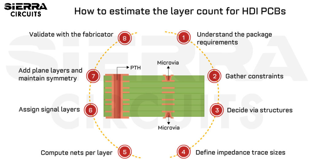
Broadly, the manufacturing yields of HDI designs for which a material is specified are determined by whether a material is dimensionally stable, susceptible to or resistant to copper migration such as conductive anodic filament (CAF) growth, able to withstand multiple laminations, and able to be laser drilled with consistent good results.
A circuit whose response remains relatively flat over its frequency range will faithfully propagate signals without distortion. The dielectric constant (Dk or Er) of a material decreases as frequency increases. High-speed digital signals involve broad bands of frequencies and thereby are subject to distortion caused by impedance variations resulting from changes in the Dk of board materials with frequency. Changes in the dissipation factor (Df) of board materials with frequency degrade signal integrity as well. Materials whose Dk and Df are low and vary little across the frequency domain of a circuit propagate signals faster and maintain signal integrity better than materials with higher Dk and Df.
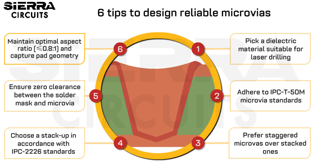
Suppose you’ve ruled out dielectrics in the FR-4 category because their Dk and Df values are too high and vary too much over the signal spectrum of your circuit. Suppose as well that your board will incorporate several high-speed devices in BGAs, each with a dense pin matrix that will require via-in-pad routing. Your design will therefore involve blind microvias and require a material thin enough that the aspect ratio of those laser-drilled vias does not exceed 0.8:1 or plating could become difficult. Remember, at a given Dk, the thinner the substrate, the narrower the traces must be to maintain a 50-ohm impedance. You’ll favor materials that have a low Dk so trace width can be wide enough to be easily manufactured and provide the necessary impedance value.
High-Speed PCB Design Guide
8 Chapters - 115 Pages - 150 Minute ReadWhat's Inside:
- Explanations of signal integrity issues
- Understanding transmission lines and controlled impedance
- Selection process of high-speed PCB materials
- High-speed layout guidelines
Download Now
Comparing Isola FR408HR, Nelco N4000-13 SI, and Panasonic Megtron 6
Let’s say a Dk under 3.7 at 1 GHz is acceptable and you’ve decided Isola FR408HR, Nelco N4000-13 SI, and Panasonic Megtron 6 are prospects, based on their data sheets. I choose these three materials, which my fabrication company deals with routinely, to illustrate my point about hidden manufacturing issues, yield, and ultimate PCB cost.
FR408HR has a higher dielectric constant and higher loss factor than both N4000-13 SI and Megtron 6, but it is cheaper in price. The Nelco 4000-13 series of materials, and in particular N4000-13 SI, have excellent electrical properties for high-speed digital applications. The SI (signal integrity) material is based on a glass cloth specially formulated to have a very low Dk over a wide frequency range that is closely matched to the Dk of its resin. Megtron 6 incorporates a unique low- Dk fabric known as flat glass. Unlike FR408 HR and N4000-13 SI, in which resin resides throughout the glass fabric weave, its resin is essentially a “butter coat” evenly distributed across the woven flat-glass fabric surface. Megtron 6 has a slightly higher average Dk value than Nelco 4000-13 SI, from 1 GHz to 10 GHz, but a much lower Df. It is somewhat more expensive than the Nelco material and is often used for RF and microwave applications, as well as for high-speed digital circuits.
The three products are comparable on paper (all are widely employed for high-speed digital PCBs), but they have quite different manufacturing characteristics when used for HDI board designs.
There are three key qualities a material must possess for HDI fabrication. First, it must be dimensionally stable, a quality that, of course, applies to non-HDI construction as well. All materials shrink and stretch to some extent during manufacturing processes, and patterning must be scaled to compensate, which is not an issue provided the material movement is predictable. Second, the material must be easily machinable: For HDI that means it can be laser drilled without problems. Third, a material must be able to survive multiple laminations. Let’s restrict this comparison of manufacturability to laser drilling, with regard to the three materials.
The word drill is really a misnomer to describe how a laser makes holes. A better term would be vaporization. Highly concentrated energy is directed in a focused beam on a specific area, which is absorbed by the material until it vaporizes. The energy must be carefully controlled to ablate material to form a hole without destroying the landing pad beneath. However, dielectric constituents absorb energy at different rates, and it is in this respect that N4000-13 SI, FR408HR, and Megtron 6 differ in manufacturability.
The Importance of Communicating with PCB Manufacturers
Let me interject a disclaimer: Though my company has extensive experience with the three materials, that experience isn’t quantified and therefore must be considered subjective. There’s no bias toward one rather than the others, except for HDI from manufacturing experience. We’ll build whatever a customer wants, if it can be constructed. The point to bear in mind is simply this: If a board is challenging to build in limited, prototype quantities, it will be no less challenging to manufacture in production runs. To repeat, yield drives profit.
My company has found that achieving clean laser-drilled holes in the Nelco material and in FR408HR requires more effort compared to creating them in Megtron 6. The resin in the Nelco fabric burns off at a much different rate than the glass fibers and too much energy is required to consume all the fibers in the hole without compromising the surrounding dielectric and the landing pad itself. FR408HR is less prone to have glass fibers protrude from hole walls than is N4000-13 SI but is less predictable in that respect. Glass bundles extend in perhaps only 5% of the holes but such inconsistency itself complicates processing. The flat glass fabric of Megtron 6 can be ablated cleanly by contrast to the other two materials, in our experience.
Nelco is continually investigating resin formulations, glass, and fabric constructions that would improve the manufacture of HDI architectures. The firm recently introduced a new material, N4800-20 SI, which it recommends in place of N4000-13 SI for HDI PCB manufacture. My company is evaluating that material and anticipates better results.
The upshot of all this is that you should consult your board manufacturer at the outset of design to identify materials that would provide the optimum balance of price, manufacturability, and performance based on your construction. I’ll dedicate this column as the first installment regarding materials and manufacturability. The next one will regard materials with the highest electrical performance for digital high-speed circuits, and for RF and microwave applications.
HDI PCB Design Guide
5 Chapters - 52 Pages - 60 Minute ReadWhat's Inside:
- Planning your stack-up and microvia structure
- Choosing the right materials
- Signal integrity and controlled impedance in HDI
- Manufacturing considerations for higher yields
Download Now
About Amit Bahl : Amit Bahl, widely recognized as the PCB Guy, earned his Bachelor of Science in Engineering from UCLA. He is currently the Chief Revenue Officer at Sierra Circuits, where he continues to lead efforts to simplify the PCB design journey and support designers and engineers in creating high-quality boards.


