


Contents
Mythbusting the Semi-Additive Process
Prudent PCB designers used to have good reasons for avoiding trace widths and spaces smaller than 3 mils beyond very short spans. But the 3 mil limitation is now becoming a thing of the past, thanks to the use of semi-additive fabrication by some board manufacturers. The main reason designers steered clear of sub 3-mil lines and spaces for more than short distances is etch factor.
The closer a trace cross-section matches an ideal rectangle, the closer it comes to matching the characteristic impedance desired by the PCB designer.
The convergence of ever-greater circuit density and ever-higher data rates has reached the point where the chemistry of conventional PCB fabrication processes cannot be controlled tightly enough to consistently satisfy design needs. The traditional manufacture of PCBs begins with a laminate clad with copper on one or both sides. PCB manufacturers purchase clad laminates (cores) from suppliers in a wide range of substrate materials and copper thicknesses, and they also create laminates by bonding substrate materials in prepreg form with copper foils in a press.
Basically, traces are patterned by applying an etch resist to the copper surface, curing the resist by selectively exposing it to light where copper should be retained as traces and other features, and then etching away (subtracting) the unexposed resist and underlying copper in an acid bath. The objective is to produce traces whose cross-section is rectangular. However, the bath not only removes copper in the vertical direction but also eats some of it away at the sides of the traces horizontally underneath the resist, resulting in the sort of profile illustrated in Figure 1.
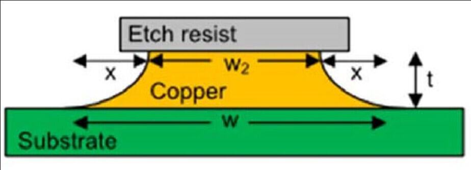
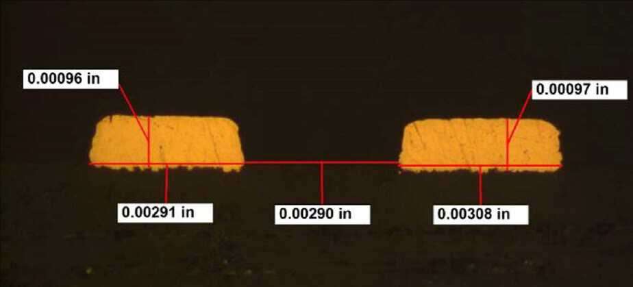
A well-controlled subtractive process repeatedly produces traces that are approximately trapezoid in cross-section, whose sides are at a 25– 45 degree included angle from the base, while the base is at design width. But bath chemistry can vary and traces can be over-etched, further diminishing their cross-section such that their top surface is much narrower than the base. The ratio between the height of the trace post-etch (t) and how far the trace has been eaten away at the top of an edge (x) is the etch factor (F). The higher the etch factor, the better the trace section resembles an ideal rectangle, provided the base is at design width. Bath chemistry can also vary such that too little copper is removed and traces at their base extend beyond design width.
At best with the subtractive process, the width of a trace at the top and at the base can be held to within 0.5 mil of design value. Such a tolerance has little consequence when traces and spaces are 3 mils or wider and signal edge rates are low. However, it has a significant effect on the characteristic impedance of thinner traces and a profound influence if those narrow traces are tightly coupled differential pairs in high-speed digital circuits. Moreover, the smaller the area of a trace cross-section is compared to an ideal rectangle, the worse the IR loss becomes along the trace. The closer a trace cross-section matches an ideal rectangle, the closer it comes to matching the characteristic impedance desired by the PCB designer.
If traces could be fabricated at design width with nearly vertical sides, the maximum circuit density could be achieved, signal integrity could be ensured, and PCB yields could be optimized. That is the case with the semi-additive fabrication process.
In contrast to the trace geometries that result from the subtractive process, which are chemistry- and process-defined, the trace geometries from the semi-additive process are lithographically defined. Photolithography creates a well-defined trace. Trace width and spaces produced by the semi-additive process are extremely close or identical to the as-designed dimensions.
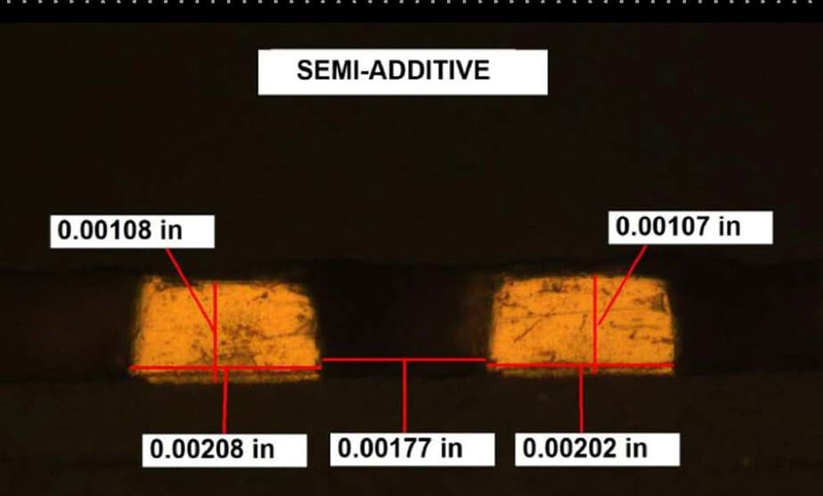
The semi-additive process is essentially the opposite of the subtractive PCB fabrication process. It starts with a laminate that is clad with much thinner copper than the thinnest conventional foils. For example, quarter-ounce copper is approximately 8.5 µm thick, but the ultra-thin foil is typically 2 µm or 3 µm thick. Such ultra-thin foils have a backing that is removed after the foil is laminated to the substrate. The holes are drilled and then a bath of electroless copper coats the bores and the foil surface. A “reverse” resist is applied, developed, and selectively removed to expose only the areas that will become the traces, vias, and other conductive features. Those exposed areas are plated up, the resist is stripped, and the ultra-thin copper remaining in the well between the conductors is etched away.

The plated-up traces and features are far more accurately defined than those produced by even the most-well-controlled subtractive processes (Figures 2 and 3). Trace width and spacing down to 1.25 mils can be maintained over distance within extremely tight tolerance. There is no penalty in manufacturing time. The semi-additive process frees designers who would otherwise be challenged to breakout dense fine-pitch BGAs and also enables very strict impedance control to ensure signal integrity.
And finally, while I have the chance to dispel myths harbored by some PCB designers, let me clear up another misconception. If any manufacturer tells you there’s a setup charge for board fabrication or assembly, tell them no thanks, you’ll shop elsewhere.
Remember, no special jigs or one-off fixtures are necessary to build these boards. Tell them I said so.

High-Speed PCB Design Guide
8 Chapters - 115 Pages - 150 Minute ReadWhat's Inside:
- Explanations of signal integrity issues
- Understanding transmission lines and controlled impedance
- Selection process of high-speed PCB materials
- High-speed layout guidelines
Download Now
About Amit Bahl : Amit Bahl, widely recognized as the PCB Guy, earned his Bachelor of Science in Engineering from UCLA. He is currently the Chief Revenue Officer at Sierra Circuits, where he continues to lead efforts to simplify the PCB design journey and support designers and engineers in creating high-quality boards.


