Speak to an Account Manager
![]() +1 (800) 763-7503
+1 (800) 763-7503
Related Categories — High Current » PCB Design » PCB Layout
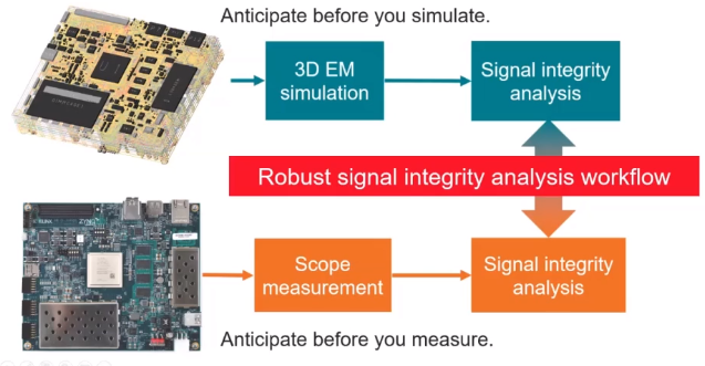
Unlock Your Signal Integrity Analysis Potential
Signal integrity analysis provides the measurement of the amount of signal degradation when the signal travels from the driver to the receiver. In other words, it signifies the signal’s ability to propagate along PCB traces without distortion.
PCB Design
PCB Via Design Using Altium Designer
The early days of PCB fabrication saw the exclusive use of through-hole vias that span the complete thickness ... more »
PCB Design
What is the Use of a Decoupling Capacitor?
System noise has become a critical issue for both analog and digital devices. The requirement for speedy interfaces ... more »
PCB Design
Unlock Your Signal Integrity Analysis Potential
Signal integrity analysis provides the measurement of the amount of signal degradation when the signal travels from the ... more »
PCB Design
PCB Via Design Using Altium Designer
The early days of PCB fabrication saw the exclusive use of through-hole vias that span the complete thickness ... more »
PCB Design
What is the Use of a Decoupling Capacitor?
System noise has become a critical issue for both analog and digital devices. The requirement for speedy interfaces ... more »
PCB Design
What is a Pad in PCB Design and Development?
The quality of a circuit board assembly depends on several factors such as the interface between the board ... more »
PCB Design
Losses in PCB Transmission Lines
A PCB transmission line comprises at least two conductors – one for the signal and another for its ... more »
PCB Design
What’s the Meaning of Schematic Diagram?
A schematic diagram is a fundamental two-dimensional circuit representation showing the functionality and connectivity between different electrical components. ... more »
PCB Design
PCB Material Selection: Electrical and Manufacturing Considerations
When it comes to PCB material selection, making the right choice for your design is important because materials ... more »
PCB Design
How to Reduce Parasitic Capacitance in PCB Layout
A PCB consists of several parallelly spanned conductors, say traces, separated by an insulator. These traces, along with ... more »
PCB Design
What Is PCIe (PCI Express)?
Innovation in computing is an ongoing trend that keeps growing exponentially in today's digital world. With data transfer ... more »
PCB Design


Fabrication, Procurement, & Assembly. PCBs fully assembled in as fast as 5 days.
- Bundled together in an entirely-online process
- Reviewed and tested by Engineers
- DFA & DFM Checks on every order
- Shipped from Silicon Valley in as fast as 5 days

Fabrication. Procurement & Assembly optional. Flexible and transparent for advanced creators.
- Rigid PCBs, built to IPC-6012 Class 2 Specs
- 2 mil (0.002″) trace / space
- DFM Checks on every order
- 24-hour turn-times available

Complex technology, with a dedicated CAM Engineer. Stack-up assistance included.
- Complex PCB requirements
- Mil-Spec & Class 3 with HDI Features
- Blind & Buried Vias
- Flex & Rigid-Flex boards