Speak to an Account Manager
![]() +1 (800) 763-7503
+1 (800) 763-7503
Related Categories — PCB Design » Via
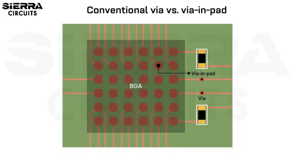
How to Use Via-in-Pad for PCB Design and Manufacturing
Multi-layered printed circuit board design requires a means to establish connections between various layers. This is done using vias ranging from through-hole vias to via-in-pad technology. While traces serve as horizontal connection elements, vias function as vertical connection elements, enabling signal and power to travel between board layers.
PCB Design
How PCB Vias Interconnect Circuit Board Layers
To achieve this criterion, PCBs are made up of multiple layers. But how are these multilayers connected to ... more »
HDI / Blind & Buried Vias
Signal Integrity: Via Stubs and Their Effects on Signal Attenuation and Data Transfer Rates
First, let's start with a few things to know about signal integrity and via stubs. A via stub ... more »
PCB Design
How to Use Via-in-Pad for PCB Design and Manufacturing
Multi-layered printed circuit board design requires a means to establish connections between various layers. This is done using ... more »
PCB Design
How PCB Vias Interconnect Circuit Board Layers
To achieve this criterion, PCBs are made up of multiple layers. But how are these multilayers connected to ... more »
HDI / Blind & Buried Vias
Signal Integrity: Via Stubs and Their Effects on Signal Attenuation and Data Transfer Rates
First, let's start with a few things to know about signal integrity and via stubs. A via stub ... more »
PCB Design


Fabrication, Procurement, & Assembly. PCBs fully assembled in as fast as 5 days.
- Bundled together in an entirely-online process
- Reviewed and tested by Engineers
- DFA & DFM Checks on every order
- Shipped from Silicon Valley in as fast as 5 days

Fabrication. Procurement & Assembly optional. Flexible and transparent for advanced creators.
- Rigid PCBs, built to IPC-6012 Class 2 Specs
- 2 mil (0.002″) trace / space
- DFM Checks on every order
- 24-hour turn-times available

Complex technology, with a dedicated CAM Engineer. Stack-up assistance included.
- Complex PCB requirements
- Mil-Spec & Class 3 with HDI Features
- Blind & Buried Vias
- Flex & Rigid-Flex boards