Speak to an Account Manager
![]() +1 (800) 763-7503
+1 (800) 763-7503
Related Categories — PCB Design » PCB Layout
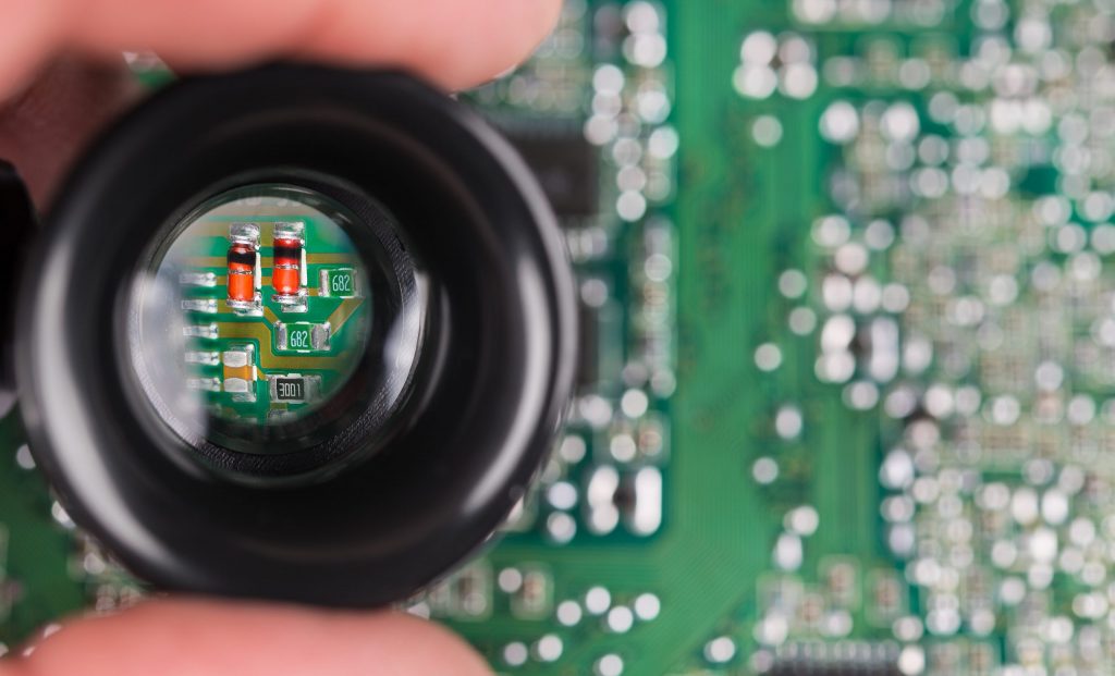
Choosing Smaller Footprints for HDI Design
The main agenda of using HDI technology is to pack more components on a smaller board. Choosing smaller footprints for HDI increases board functionality and component density.
HDI / Blind & Buried Vias
Top 6 Missing Information When Requesting a PCB Quote
Once a circuit board designer prepares the design, the next step is to find a manufacturer to transform ... more »
PCB Assembly
Impedance Matching in HDI PCB Design
Impedance matching is the way of configuring the input impedance of a load or the output impedance of ... more »
Controlled Impedance
Choosing Smaller Footprints for HDI Design
The main agenda of using HDI technology is to pack more components on a smaller board. Choosing smaller ... more »
HDI / Blind & Buried Vias
Top 6 Missing Information When Requesting a PCB Quote
Once a circuit board designer prepares the design, the next step is to find a manufacturer to transform ... more »
PCB Assembly
Impedance Matching in HDI PCB Design
Impedance matching is the way of configuring the input impedance of a load or the output impedance of ... more »
Controlled Impedance
What Should a PCB Fab Drawing Include?
A fab drawing is one of the different file types that convey the manufacturing details of a printed ... more »
PCB Design
Mastering the Art of PCB Design Basics
To be a proficient designer, understanding the basics of PCB design is vital. The knowledge of appropriate component ... more »
PCB Design
Significance of Electromagnetic Field Solvers
Electromagnetic fields are part of the spectrum ranging from static magnetic fields to high-intensity gamma rays. These fields ... more »
PCB Design
How to Build a Flex Stack-Up with Controlled Impedance
Impedance is the measurement of the restriction imposed by a circuit on the current flow. It is similar ... more »
Controlled Impedance
How to Reduce Signal Attenuation in High-Speed PCBs
Signal attenuation is the most prevalent term when high-speed signals propagate on a circuit board. It is one ... more »
High Speed
What is a Bill of Materials in PCB Design?
Before we start any project, it is a good habit to make a list of all the components ... more »
PCB Assembly


Fabrication, Procurement, & Assembly. PCBs fully assembled in as fast as 5 days.
- Bundled together in an entirely-online process
- Reviewed and tested by Engineers
- DFA & DFM Checks on every order
- Shipped from Silicon Valley in as fast as 5 days

Fabrication. Procurement & Assembly optional. Flexible and transparent for advanced creators.
- Rigid PCBs, built to IPC-6012 Class 2 Specs
- 2 mil (0.002″) trace / space
- DFM Checks on every order
- 24-hour turn-times available

Complex technology, with a dedicated CAM Engineer. Stack-up assistance included.
- Complex PCB requirements
- Mil-Spec & Class 3 with HDI Features
- Blind & Buried Vias
- Flex & Rigid-Flex boards