Related Categories — PCB Assembly » PCB Design » PCB Layout
How to Design Reliable Microvias in Your PCBs
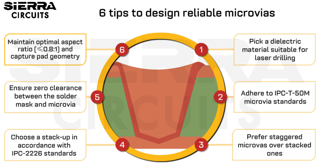
Key design strategies for enhancing microvia reliability include selecting suitable materials for laser drilling, adhering to IPC-T-50M guidelines, and implementing […]
HDI / Blind & Buried Vias
How to Pick the Right Flex PCB Materials for Your Application?
When selecting flex PCB materials, you need to consider the application type (dynamic or static), stiffener requirements, and ... more »
Flex PCBs
PCB Solder Mask Clearance Every Engineer Should Know
PCB solder mask clearance is the space between a copper pad and the surrounding solder resist. It typically ... more »
PCB Design
How to Design Reliable Microvias in Your PCBs
Key design strategies for enhancing microvia reliability include selecting suitable materials for laser drilling, adhering to IPC-T-50M guidelines, ... more »
HDI / Blind & Buried Vias
How to Pick the Right Flex PCB Materials for Your Application?
When selecting flex PCB materials, you need to consider the application type (dynamic or static), stiffener requirements, and ... more »
Flex PCBs
PCB Solder Mask Clearance Every Engineer Should Know
PCB solder mask clearance is the space between a copper pad and the surrounding solder resist. It typically ... more »
PCB Design
10 Best High-Speed PCB Routing Practices
A PCB designer has a difficult task when it comes to routing a circuit board. Things get a ... more »
High Speed
What Causes High-Leakage Current in PCBs and How to Prevent It?
High-leakage current in PCBs is caused by moisture absorption and inadequate creepage and clearance distances. You can prevent ... more »
PCB Design
Decoupling Capacitor Placement Guidelines Every PCB Designer Should Know
Decoupling is a way of isolating signal components from composite signals based on frequency. Therefore, understanding which range ... more »
PCB Layout
Designing and Fabricating Ultra-HDI PCBs
Ultra-HDI PCBs are becoming essential in high-speed applications such as AI systems, where circuit density and signal integrity ... more »
HDI / Blind & Buried Vias
What is ITAR, the International Traffic in Arms Regulations?
Think about the technology that your company has developed recently and planning to have a patent. You are ... more »
Defense & Space
PCB Stack-up: Plan, Design, Manufacture and Repeat
Often ignored, it is important to understand the difference between an HDI stack-up and a standard stack-up. The ... more »
PCB Design
Fabrication, Procurement, & Assembly. PCBs fully assembled in as fast as 5 days.
- Bundled together in an entirely-online process
- Reviewed and tested by Engineers
- DFA & DFM Checks on every order
- Shipped from Silicon Valley in as fast as 5 days
Fabrication. Procurement & Assembly optional. Flexible and transparent for advanced creators.
- Rigid PCBs, built to IPC-6012 Class 2 Specs
- 2 mil (0.002″) trace / space
- DFM Checks on every order
- 24-hour turn-times available
Complex technology, with a dedicated CAM Engineer. Stack-up assistance included.
- Complex PCB requirements
- Mil-Spec & Class 3 with HDI Features
- Blind & Buried Vias
- Flex & Rigid-Flex boards


