


Contents
The topic of the clock’s power supply jitter performance seems to be a current focus of clock, ADC, and power supply, manufacturers. The reasoning is clear; clock jitter interferes with the performance of digital circuits including high-speed ADCs. High-speed clocks can be quite sensitive to the “cleanliness” of the power they receive, though quantifying the relationship takes some effort.
Many voltage regulator manufacturers are developing new lines of regulators (predominantly LDOs) that promise higher PSRR specifically for powering precision clocks and sensitive circuits. There have also been recent articles showing the performance of the clock and subsequent high-speed ADCs can be quite acceptable when the linear regulator is replaced with a switching regulator.[i]
The test setup for measuring clock phase noise and power supply jitter is shown in Figure 1:
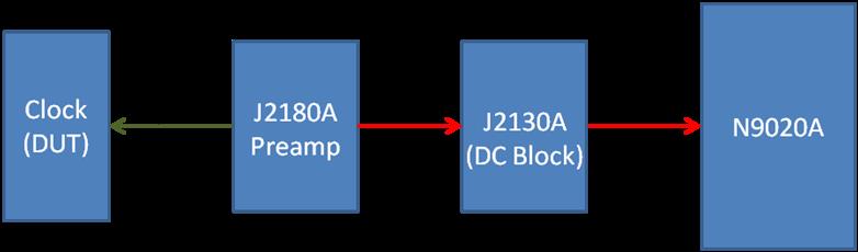
Noise paths to the clock
The most fundamental relationship between the clock jitter, Tj, and the power supply noise, Nv, can be defined by Equation 1.

This relationship makes it clear that there is a need to establish the sensitivity of the clock jitter to the power supply jitter as a function of frequency. It is also important to understand the frequency range of interest, which generally extends to the highest signal frequencies the ADC will operate at. Not all clocks are similar and some of the newer, higher-performance clocks have built-in high-performance linear regulators, and Phase Lock Loops (PLLs) cleaners in order to reduce the sensitivity of the clock performance to the power supply jitter.
Defining the power supply noise requires at least three terms, though there can be several less prominent paths as well.
The relationships in Equation 2 show the three major noise paths to the clock. The first is the noise presented at the input to the linear regulator, which is reduced by the Power Supply Rejection Ratio (“PSRR”) of the regulator. This illustrates why so many manufacturers are working to improve the high-frequency PSRR of next-generation LDOs. The second noise path is from the regulator’s internal noise to the regulator’s output. The third and less frequently discussed path is due to current variations at the output of the linear regulator interacting with the impedance present at the output of the regulator, which is also the input power to the clock. This is especially significant if other dynamic loads are connected to the same regulator.

One of the more complex issues associated with measuring a clock’s performance is determining and then presenting the clock with appropriate noise voltages and currents. This is a major shortcoming in some of the recently published articles on the subject[i].
This article will demonstrate the effects of and the sensitivities to these noise paths, as well as provide some general guidelines for streamlining the power requirements in order to optimize the performance of the clock.
Also read: The Pros and Cons of Composite Amplifiers

Measuring the Noise
For the examples in this article, we are using a low-cost, off-the-shelf, 3.3V, 125MHz CMOS SMD clock. This frequency is low enough to be fairly common and relatively inexpensive while offering a sensitivity that is high enough to be interesting. Since the CMOS oscillator is designed to operate into a 15pF load, a 10X scope probe is used along with a Picotest J2180Awideband preamplifier to convert the high impedance probe to the 50 Ohm input of the Agilent N9020A Signal Analyzer we are using to measure the clock noise. Due to its popularity, we are using an LM317 linear regulator, as well as a custom-designed voltage regulator to provide power to the clock for the test. A Picotest Voltage Regulator Test Standard or “VRTS” kit is used as the test bed since it provides simple connections to the inputs and outputs, as well as supporting interchangeable linear regulators for comparative measurements.
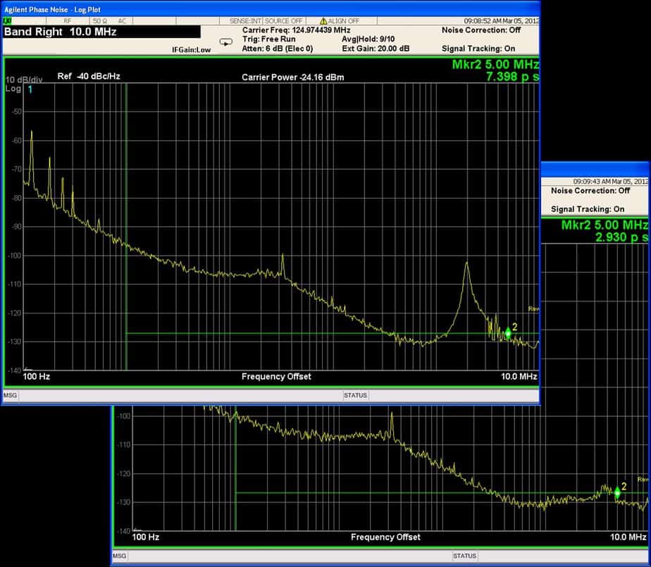
The large 2MHz signal from the LM317 seen in Figure 2 is due to the control loop of the regulator and the impedance of the wall adapter, including the impedance of its output wires and connector. The custom-designed regulator, offering 50dB PSRR at 2MHz, as well as much higher bandwidth, rejects most of this input noise signal.
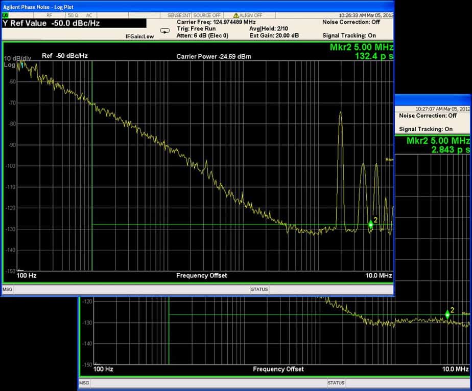
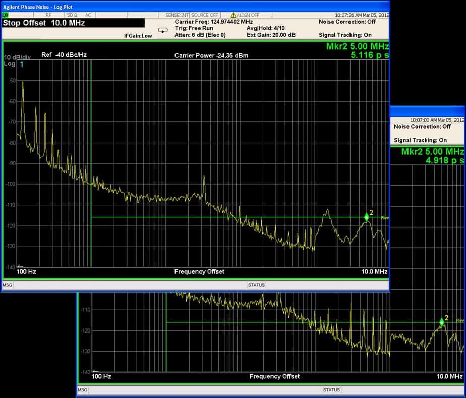
Replacing the wall adapter with a benchtop supply that is connected to the VRTS board with a common 18” banana test leads significantly degrades the performance of the clock as shown in Figure 3. While the test leads and the wall adapter both measure approximately 1uH of inductance, the bench supply impedance, and test leads result in a much higher Q (and, in fact, is oscillating as can be seen by the appearance of the 2MHz signal and its harmonics ). The addition of a 0.47uF ceramic capacitor at the input to the regulator greatly reduces the input impedance at 2MHz. The resulting jitter is reduced to 2.8pS.
The replacement of the wall adapter with a bench supply and input capacitor decoupling greatly reduced the power supply jitter. In order to demonstrate the sensitivity of the clock to the input and output impedances of the power circuitry, a Picotest J2111A Current Injector is used to provide a narrow current pulse that can be connected at either the input or output of the linear regulator, providing external transient stimulus. The narrow pulse is rich in harmonics.

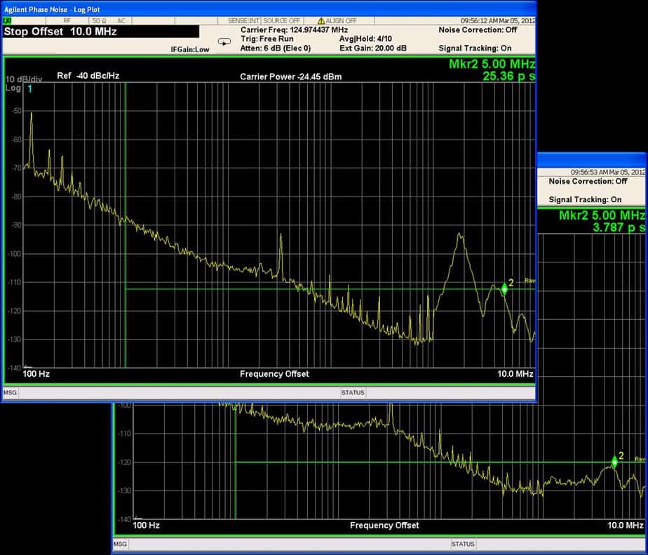
In Figure 4 the J2111A current pulse is connected to the input of the linear regulator. The finite impedance of the wall adapter transforms the current signal to a voltage spectrum, which then passes through the linear regulator via PSRR and onto the clock, producing a jitter. The addition of the capacitor reduces the impedance, and therefore, the noise voltage to the clock. It is important to be sure that the capacitor does not resonate with inductors, beads, or other circuit reactances that can result in high Q resonances, which would increase the noise level at the clock.
In Figure 5 the current pulse from the J2111A current injector is connected to the output of the linear regulator, where again the finite regulator impedance transformers this current into noise voltage that is then passed on to the clock adding jitter. It can be seen in Figure 5 that the high bandwidth custom regulator has a much lower impedance below 1MHz as evidenced by the greater reduced spur amplitudes, while the high bandwidth regulator also displays a resonance near 1.5MHz that contributes to jitter and both regulators have a resonance near 5MHz that contributes to jitter.
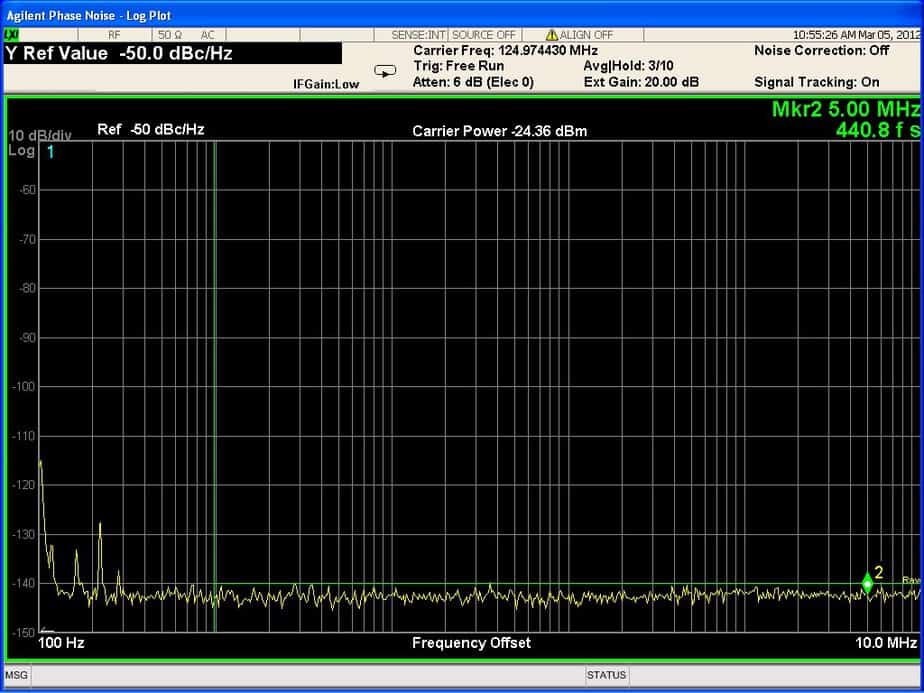
In order to assure the validity and also determine the measurement limitations, the displayed average noise level (DANL) is shown in Figure 6. The noise floor is approximately -143 dBc and the corresponding jitter is 441fS.
We have shown via a simple measurement that the clock is sensitive to the power supply jitter. We have also demonstrated that the finite non-zero impedance levels at the input and output of the regulator can greatly contribute to the clock jitter as a result of an external stimulus. While the PSRR of the linear regulator is the key term in the clock jitter sensitivity, all of the other terms also need to be considered.
A few essential design guidelines for providing power to a clock or LNA are:
- Minimize the impedances at both the input and the output of the regulator feeding the clock. This minimizes susceptibility to external signals.
- Maximize PSRR of the regulator in order to attenuate input signals as much as possible.
- Assure there are no phase discontinuities in the impedance (high Q resonances) at either the regulator input or output. These impedances should always be measured over the entire frequency range of interest.
- Be careful when using RF beads to isolate the oscillator from external noise. Beads can be quite inductive and can cause phase discontinuities which can be counterproductive. While the bead will attenuate noise from the regulator, it can also increase the impedance, making the clock more susceptible to load current induced jitter.
Lastly, do not operate any other dynamic equipment from the same regulator as the clock. The stability or phase discontinuities of any other regulators that share a common input with the clock’s regulator can result in crosstalk introducing another path to clock jitter.
Also read our article: 7 Considerations for PCB Power Supply Design
__________________________
[i] “Power-supply design for high-speed ADCs”, Thomas Neu, TI App Note, Analog Applications Journal, 1Q 2010
For more design information, check with our DESIGN SERVICE team.

High-Speed PCB Design Guide
8 Chapters - 115 Pages - 150 Minute ReadWhat's Inside:
- Explanations of signal integrity issues
- Understanding transmission lines and controlled impedance
- Selection process of high-speed PCB materials
- High-speed layout guidelines
Download Now


