Contents

On-demand webinar
How Good is My Shield? An Introduction to Transfer Impedance and Shielding Effectiveness
by Karen Burnham
KiCad is a powerful open-source PCB design tool with advanced routing features to ensure signal integrity, noise reduction, and trace layout optimization.
In this KiCad tutorial, you’ll learn the essential steps to route a PCB. We will cover critical aspects like adding ground pours, managing power routing, handling differential pairs, and applying orthogonal routing techniques.
Understanding the prerequisites for routing in KiCad
Before starting the routing process, ensure the components are placed strategically to simplify the routing process and minimize the need for vias.
For tips on efficient component placement, see component placement guidelines for PCB design and assembly.
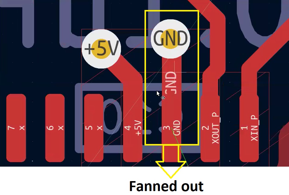
During the placement stage, complete the fan-out process, adding all the required vias. This avoids the need for additional vias during the routing phase. By managing this upfront, you’ll make the routing process much smoother and more efficient.
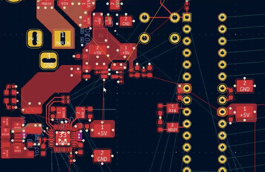
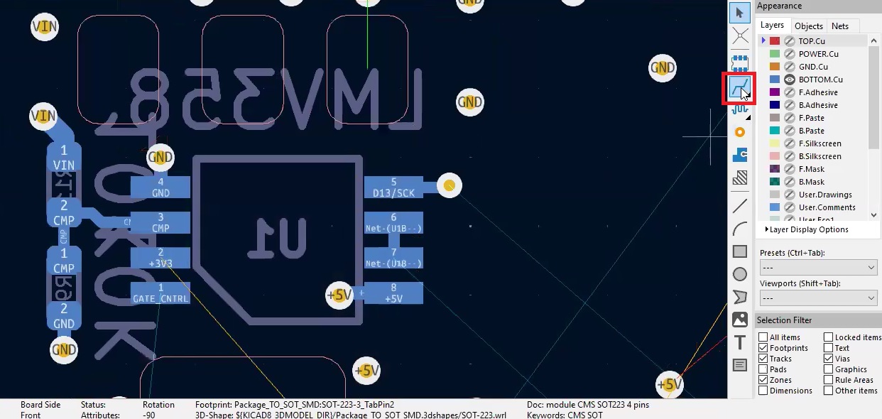
For instance, in this example, you can see that each pin with a net is fanned out. This means the necessary traces and vias are in place. Read our tutorial how to place components in KiCad for more information.
Download our KiCad 9 Step-by-Step Guide to quickly understand the PCB design workflow.

KiCad 9 Step-by-Step Guide
6 Chapters - 41 Pages - 30 Minute ReadWhat's Inside:
- A complete KiCad 9 workflow from project creation to production file generation
- Step-by-step guidance on creating custom libraries and linking symbols to footprints
- Practical design checks: ERC and DRC
- Best practices for generating a clean BOM and fabrication-ready Gerber files
Download Now
Step-by-step procedure to route a PCB in KiCad
Step 1: Add a ground pour
Follow these steps to add a ground pour in your layout:
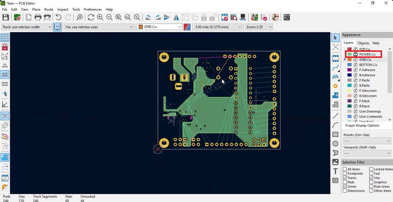
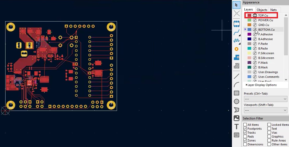
Step 1.1: Select the ground layer
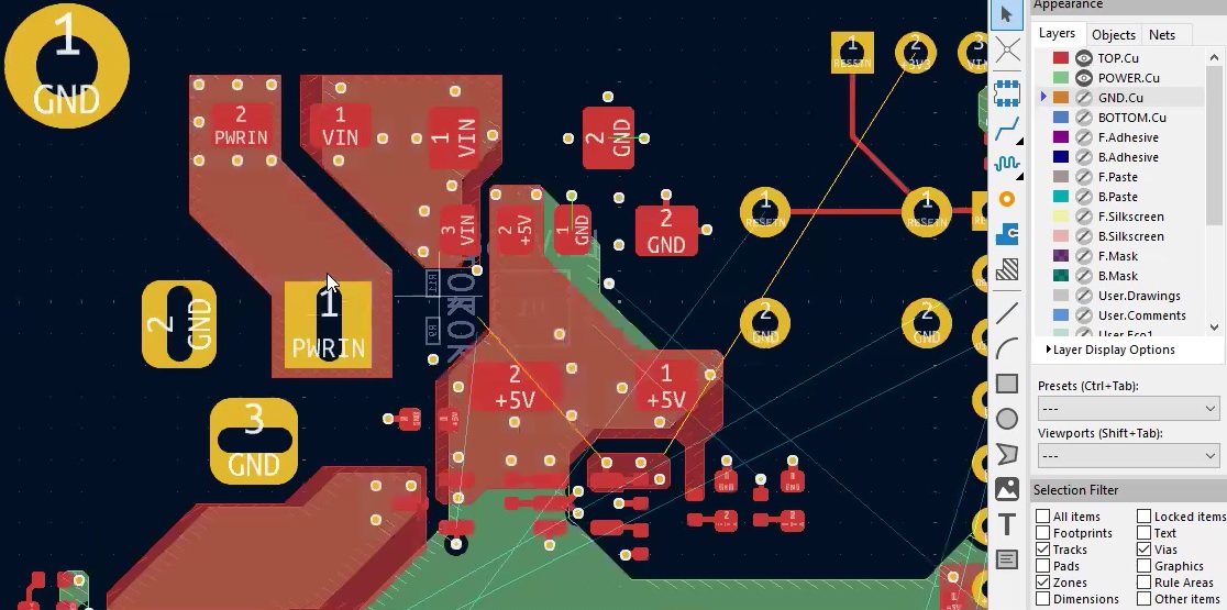
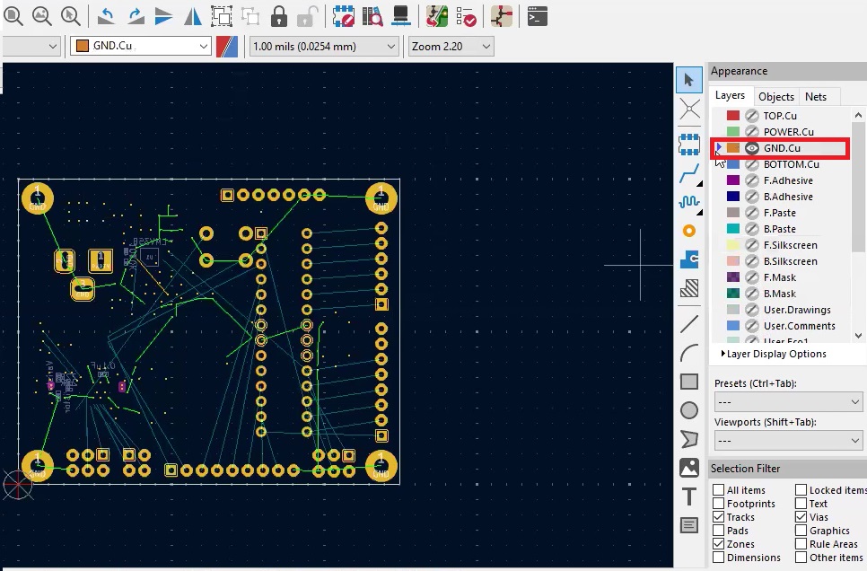
First, ensure you’re working on the correct layer. In this layout, layer 3 is a ground layer.
To select the ground layer, click GND.Cu in the Layers tab under the Appearance section.
Step 1.2: Add a filled zone
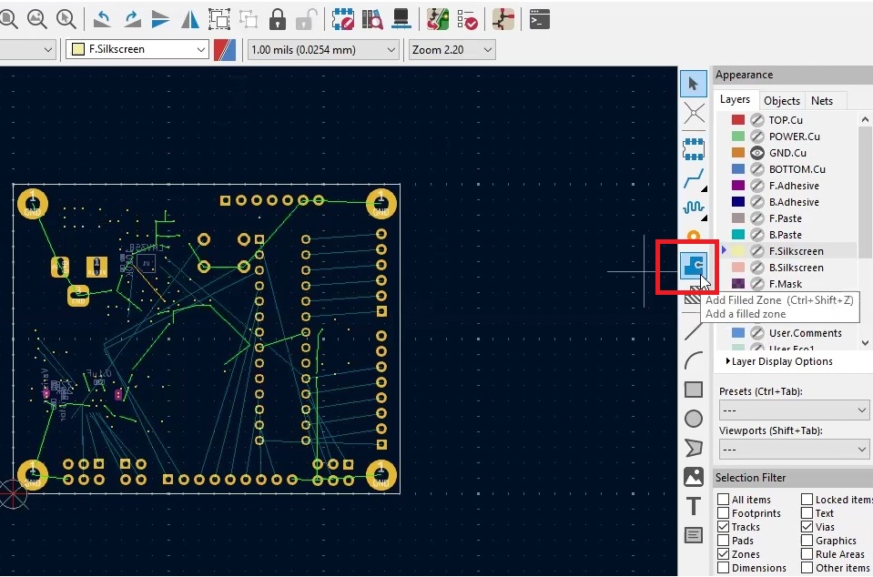
Click on Add Filled Zones in the vertical toolbar or navigate to Place –> Add Filled Zones in the top menu.
Step 1.3: Define the zone area
Before placing the zone, set the grid spacing to help you precisely place and align components and tracks on your layout.
To define the grid spacing, use the drop-down panel and set it to 5 mil.
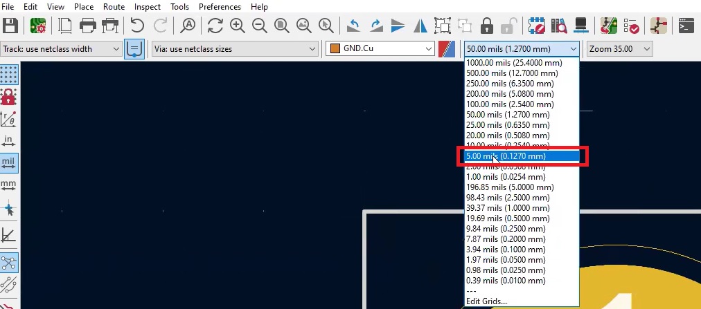
Maintain at least 20 mil spacing between the board’s edge and the zone. Measure 20 mils from the X and Y axes at the board’s edge and click to begin defining the zone.

Step 1.4: Configure copper zone properties
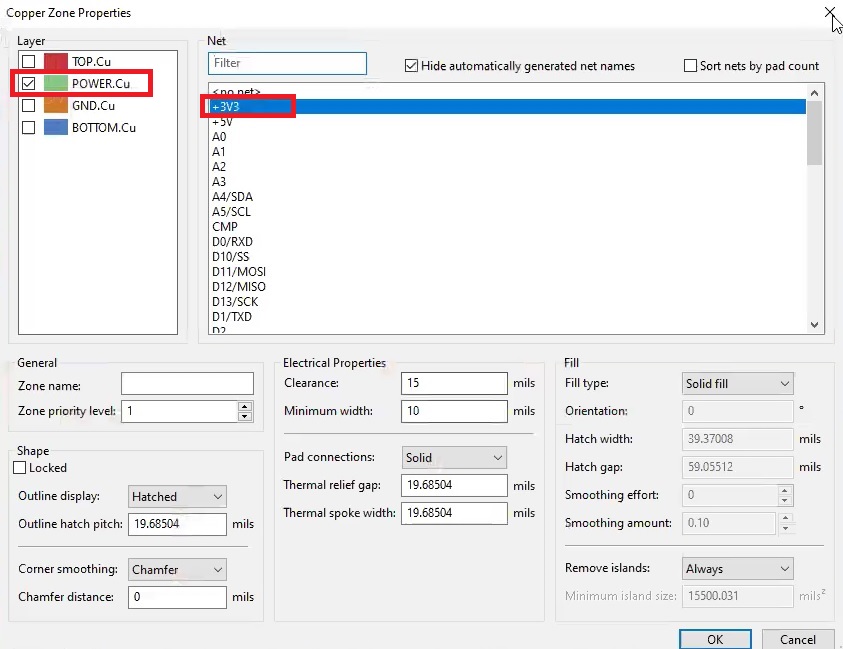
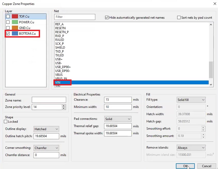
To place the zone, click on your screen. The Copper Zone Properties window will appear.
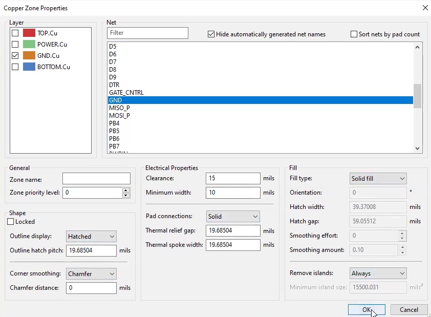
Here’s what you need to configure:
- Layer: Ensure that GND.Cu is selected.
- Net: Choose GND.
- Zone name: Optionally, you can name the zone. This can be useful if you set specific rules for this zone in the custom rules section.
- Electrical properties:
- Clearance: 15 mil.
- Minimum width: 10 mil.
- Pad connections: Choose Solid for the pad connection, as we’re not using thermal reliefs.
- Fill type: Select Solid fill for a complete pour. Hatch fill is typically used for flex PCBs, but for a rigid PCB, solid fill is preferable.
- Shape:
- Outline display: Select Hatched for the zone outline display.
- Corner smoothing: Set this to Chamfer for smoother edges.
- Remove islands: Enable this option as Always to remove any isolated copper areas after the pour automatically.
Step 1.5: Apply and fill the zone
After configuring these settings, click OK.
Next, select the area you want the ground pour to cover. Once the area is selected, right-click and choose Close Outline. Then, right-click again and select Cancel from the same menu.
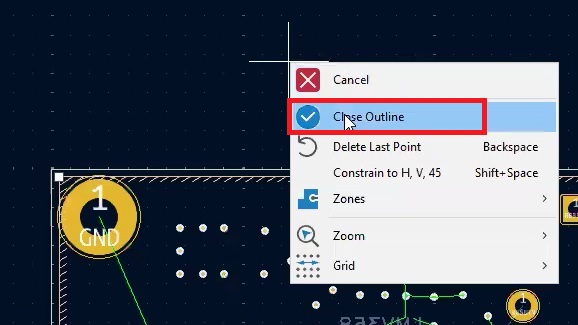
Click on the ground pour outline you’ve drawn on the PCB layout, select Zones followed by Fill All Zones to complete the ground pour.
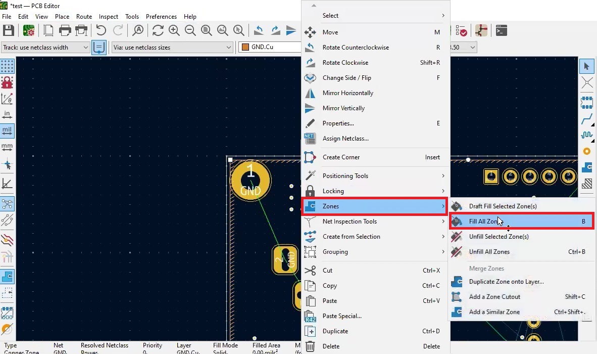
Step 1.6: Review the ground plane
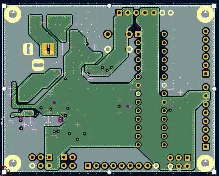
After zone filling, review the third layer. You’ll see that the entire third layer is now covered by the copper ground pour.
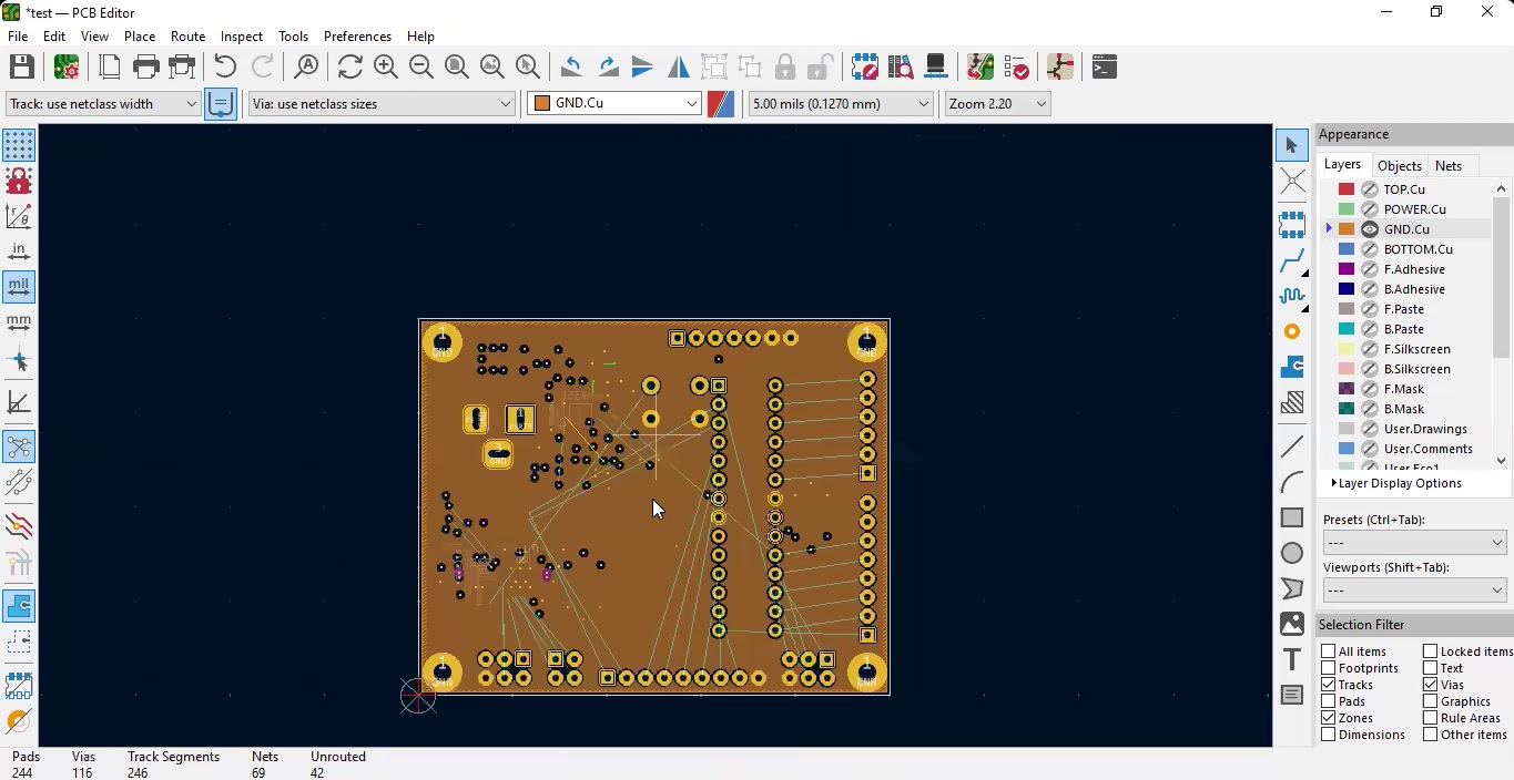
All ground vias will automatically be connected to this layer.
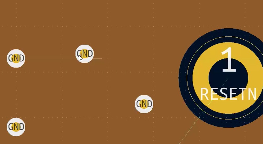
This completes the process of adding a ground plane in KiCad.
For step-by-step guidelines on designing a PCB using KiCad, download our eBook.

KiCad Design Guide
10 Chapters - 161 Pages - 180 Minute ReadWhat's Inside:
- Creating a component symbol library
- Setting up board parameters and rules
- How to route differential pairs
- How to place of components
Download Now
Step 5: Route the crystal oscillator
Another crucial part of Kicad PCB routing is crystal placement. A crystal is a continuously varying signal required for any microcontroller to operate and used as a reference signal. This should be very close to the microcontroller, and its track should be as short as possible.
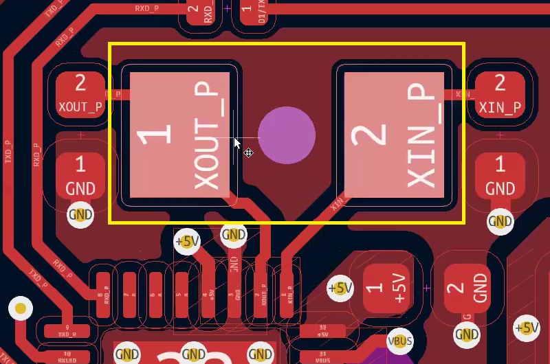
Follow these steps to route a crystal.
Step 5.1: Place the crystal close to the IC pins
Position the crystal as close as possible to the relevant IC pins. This reduces the trace length and helps maintain signal integrity. While placing the crystal, connect it directly to the IC pins using the interactive routing tool (X key) to ensure the shortest route.
Step 5.2. Position load capacitors near the crystal
Place the load capacitors close to the crystal, preferably on the same layer. If space constraints make this difficult, place them on the bottom layer directly beneath the crystal to keep them close.
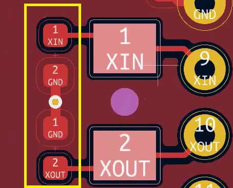
Connect the load capacitors to the ground plane through a ground via.
To place a via:
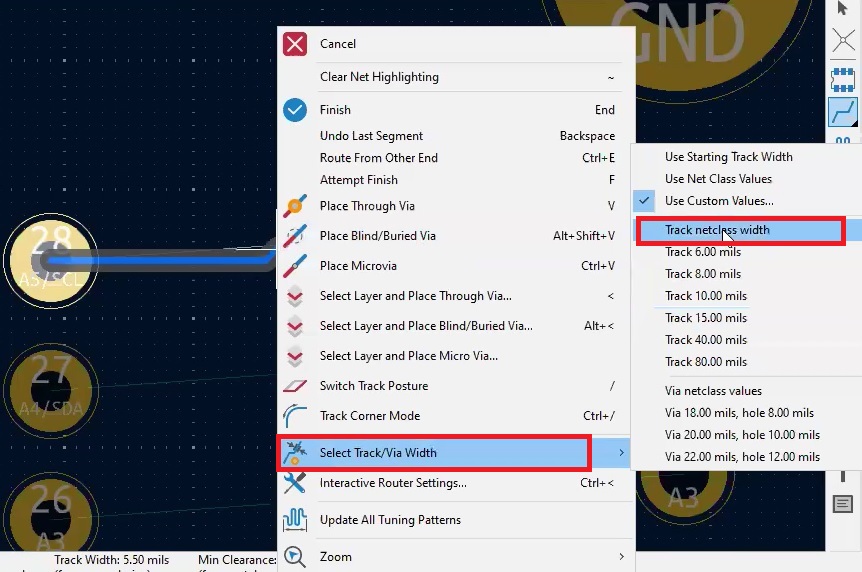
- Begin routing a track by selecting the Route Tracks (or shortcut key X)
- While routing, press the V key on your keyboard. This automatically places a via at the current cursor position and switches the routing to the next layer in the stack.
- Move the cursor to continue routing on the new layer. The via will connect the trace from the current layer to the newly selected layer.
- To stop routing, right-click and choose Cancel or press the Esc key.
The aim is to keep the crystal and its load capacitors close to each other and the IC pins to minimize signal degradation.
Step 5.3: Fan out critical power traces
Before finalizing the crystal placement, ensure critical power traces, such as 5V, are properly fanned out with vias.
Place vias to connect power traces to other layers, ensuring power distribution is handled before placing the crystal too close to the IC pins.

Step 5.4: Optimize the crystal placement
Once the power traces are fanned out, finalize the crystal’s position. Ensure it is close to the IC pins while maintaining enough clearance from power vias.
Always prioritize the placement and routing of crystals and bypass capacitors to ensure stable operation.
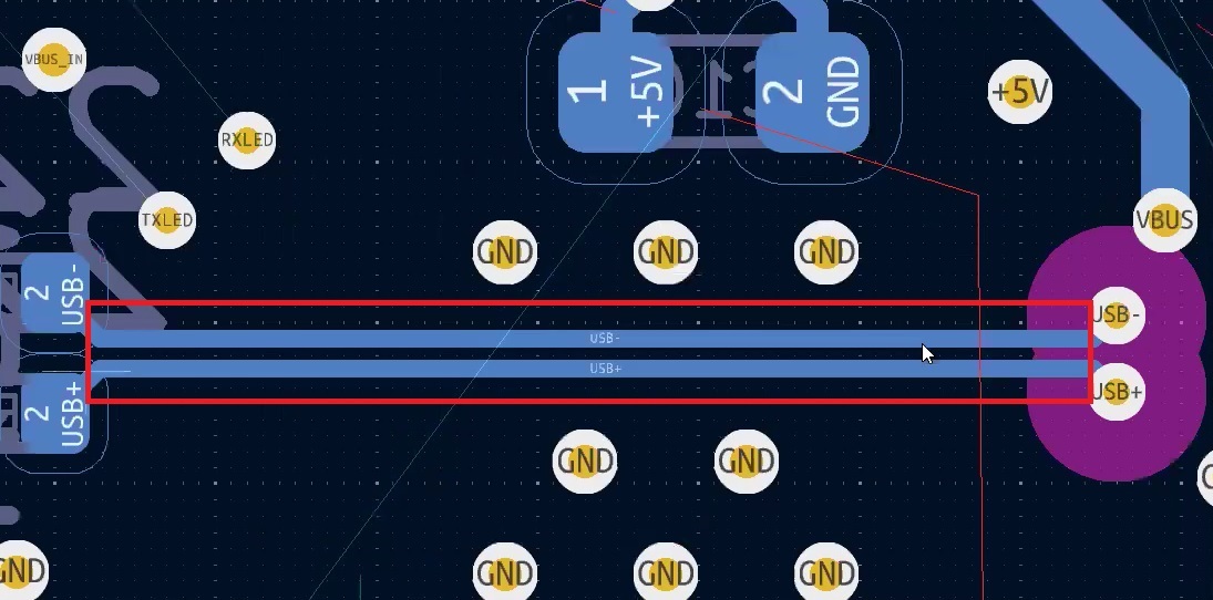
After completing the PCB routing in KiCad, check that the designators do not overlap with the differential pairs. It’s acceptable if they overlap with the tracks but not the pairs.
Step 6: Add ground pours on the outer layers
After routing, you must add ground pours on the outer layers. This is essential for providing a low-impedance return path for your signals and improving overall electromagnetic compatibility.
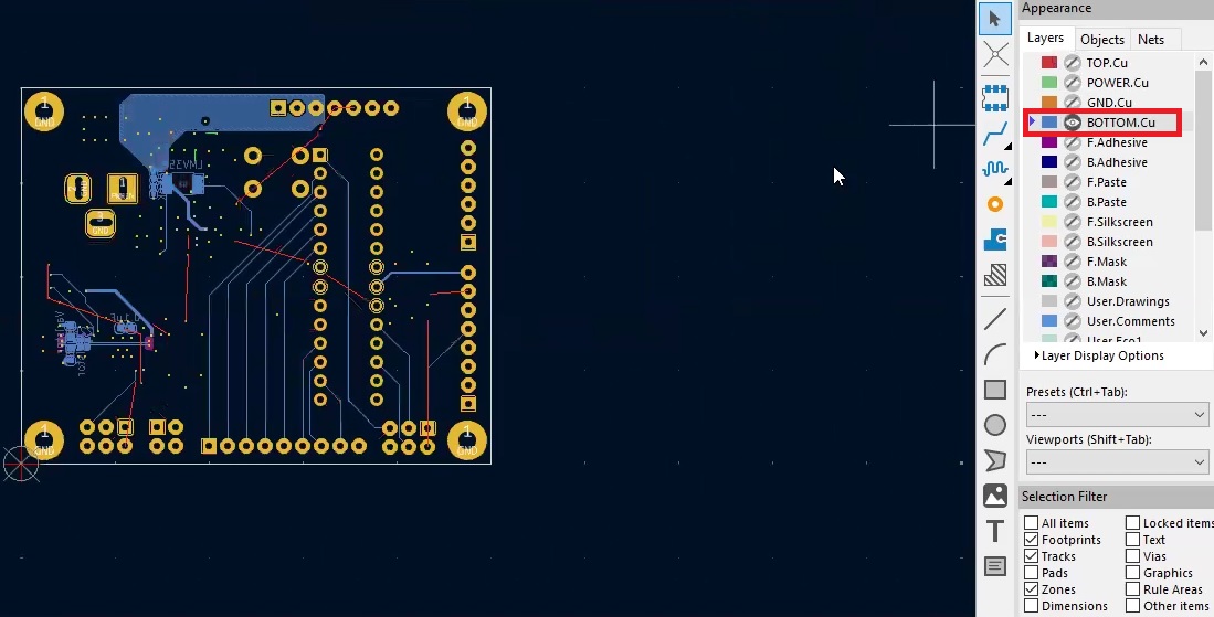
Start by pouring copper on the desired portion of the top and bottom layers. Ensure all pours are complete and consistent.
Maintain sufficient clearance between polygons and traces to avoid unintended interactions, especially around critical impedance traces. Keep a clearance of 15 mil between polygons and 10 mil between polygons and traces.
For high-impedance traces, use a clearance of 5W (five times the trace width) to avoid signal distortion.
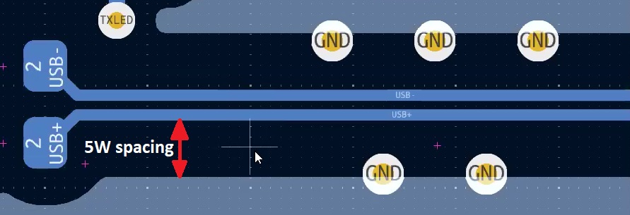
If maintaining a 5W clearance isn’t feasible, you can reduce it to 3W but avoid going any lower to prevent impedance issues.
If maintaining the required clearance isn’t possible and the copper pours significantly impact the trace impedance, it’s better to avoid pouring copper in those areas altogether.
Step 7: Adjust reference text placement and size
To move the ref text, place the cursor on it, select it, and find a suitable place. Select a proper place so the distance from the ref text is at least 6 mil from the pads.
Click Edit —> Edit Text & Graphic Properties from the menu to change the size. Choose the layer as F.Silkscreen and adjust all the required properties, then click OK.
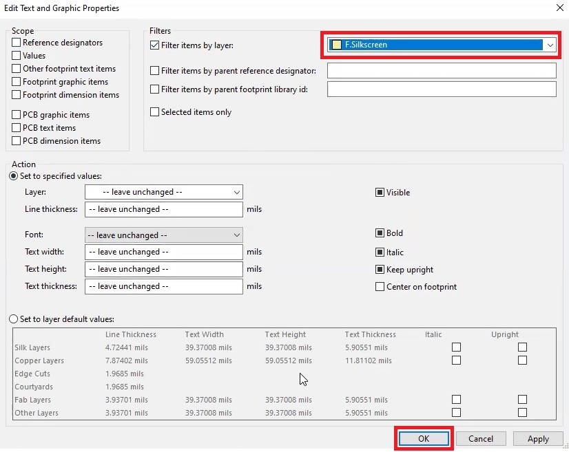
You can place your ref text over your vias if they are tented, which means they will be covered with the solder mask. Always keep ref text away from the pads and the vias. If it is impossible to keep it away from your vias, then tent your vias.
Step 8: Run design rules checker (DRC)
Let’s complete the entire placing of the ref text before starting with the DRC. Make sure that all the ref texts are away from the pins. Once this is done, you can run a DRC.
This will check whether those rules are being followed or not. It ensures no violations, such as overlapping traces or too-close clearances.
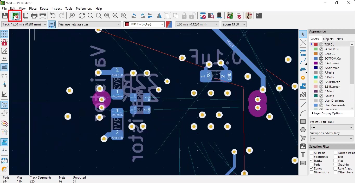
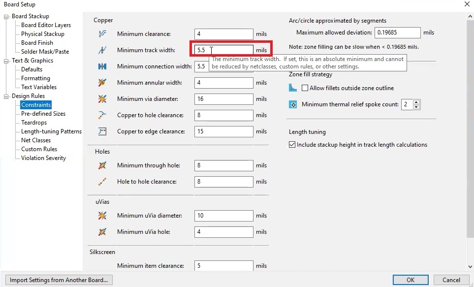
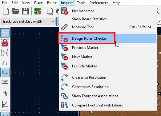
So, let’s see how it works. Save this and go to Inspect and Design Rules Checker. This is the minimum track width as per the DRC.
To create a report file:
Step 8.1: Navigate to Inspect > Design Rules Checker.
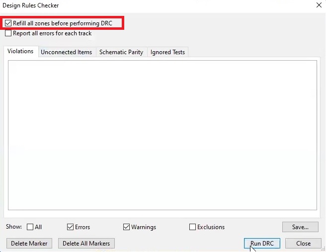
Step 8.2: Select Refill all zones before performing DRC
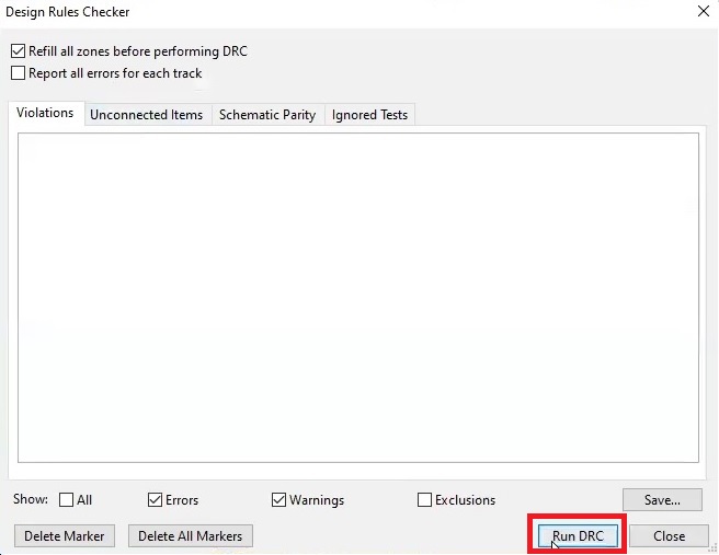
Step 8.3: Click Run DRC.
Step 8.4: Specify the report file location and click Save.
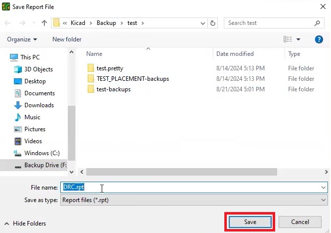
Now, the DRC tells us there are a few errors. If there are any errors in the DRC, you need to solve them before going further.
For more on DRC, see how to run design rule checks for your PCBs.
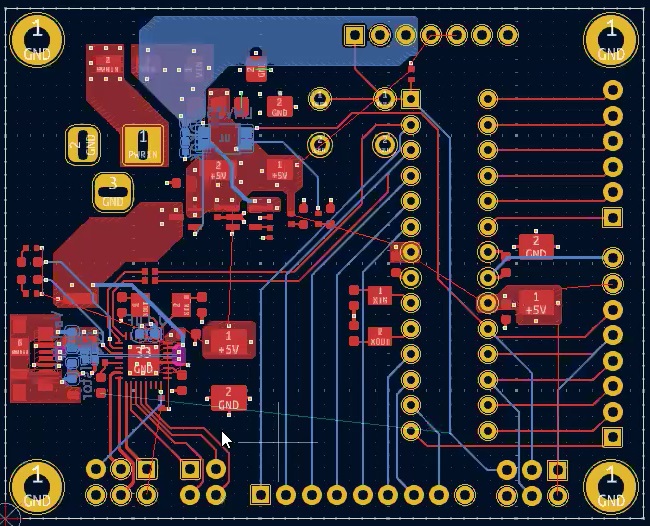
To route a PCB in KiCad, carefully plan your layout, follow design rules, and make adjustments to ensure a functional and manufacturable board.
Have queries on PCB design, assembly, and manufacturing? Post them on our forum, SierraConnect; our experts will resolve them.
About Pooja Mitra : Pooja Mitra is an electronics and communication engineer. With an experience of over three years in the PCB industry, she creates industry-focused articles that help electrical and PCB layout engineers.


