Speak to an Account Manager
![]() +1 (800) 763-7503
+1 (800) 763-7503
Related Categories — PCB Design
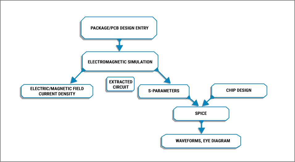
Significance of Electromagnetic Field Solvers
Electromagnetic fields are part of the spectrum ranging from static magnetic fields to high-intensity gamma rays. These fields are generated by the interaction between electric and magnetic field lines.
PCB Design
How to Reduce Signal Attenuation in High-Speed PCBs
Signal attenuation is the most prevalent term when high-speed signals propagate on a circuit board. It is one ... more »
High Speed
What is a Bill of Materials in PCB Design?
Before we start any project, it is a good habit to make a list of all the components ... more »
PCB Assembly
Significance of Electromagnetic Field Solvers
Electromagnetic fields are part of the spectrum ranging from static magnetic fields to high-intensity gamma rays. These fields ... more »
PCB Design
How to Reduce Signal Attenuation in High-Speed PCBs
Signal attenuation is the most prevalent term when high-speed signals propagate on a circuit board. It is one ... more »
High Speed
What is a Bill of Materials in PCB Design?
Before we start any project, it is a good habit to make a list of all the components ... more »
PCB Assembly
How Does Circuit Simulation Work?
PCB designers have to consider various design parameters in order to design a successful board. To ensure their ... more »
PCB Design
Unlock Your Signal Integrity Analysis Potential
Signal integrity analysis provides the measurement of the amount of signal degradation when the signal travels from the ... more »
PCB Design
PCB Via Design Using Altium Designer
The early days of PCB fabrication saw the exclusive use of through-hole vias that span the complete thickness ... more »
PCB Design
What is the Use of a Decoupling Capacitor?
System noise has become a critical issue for both analog and digital devices. The requirement for speedy interfaces ... more »
PCB Design
What is a Pad in PCB Design and Development?
The quality of a circuit board assembly depends on several factors such as the interface between the board ... more »
PCB Design
Losses in PCB Transmission Lines
A PCB transmission line comprises at least two conductors – one for the signal and another for its ... more »
PCB Design


Fabrication, Procurement, & Assembly. PCBs fully assembled in as fast as 5 days.
- Bundled together in an entirely-online process
- Reviewed and tested by Engineers
- DFA & DFM Checks on every order
- Shipped from Silicon Valley in as fast as 5 days

Fabrication. Procurement & Assembly optional. Flexible and transparent for advanced creators.
- Rigid PCBs, built to IPC-6012 Class 2 Specs
- 2 mil (0.002″) trace / space
- DFM Checks on every order
- 24-hour turn-times available

Complex technology, with a dedicated CAM Engineer. Stack-up assistance included.
- Complex PCB requirements
- Mil-Spec & Class 3 with HDI Features
- Blind & Buried Vias
- Flex & Rigid-Flex boards