Contents

On-demand webinar
How Good is My Shield? An Introduction to Transfer Impedance and Shielding Effectiveness
by Karen Burnham
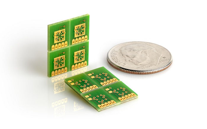
The world of electronics is about to explode or, should I say “implode,” the definition of which is “to collapse inward, violently.” This implosion will be driven by a serious size reduction or, huge improvements in the functionality of electronic products, resulting in the miniaturization of printed circuit boards. Here are a few tips that will help you understand how to handle micro PCB design and manufacturing.
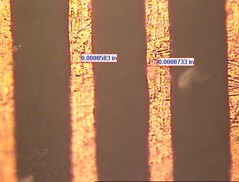
Today, the size reduction in the basic circuit board will allow designers to reduce the size of their PCBs by half or, to a quarter, the original size. We say “today,” because, as of this writing, I know of a few companies moving into microelectronic printed circuits; the very fine lines that used to be unavailable to the designers will now become mainstream, with the old absolute minimum line width of 75 microns (3 mils) giving way to 30 microns (1.2 mils) or less.
With smaller traces and vias, new design rules are required because the printed circuit manufacturing methods are quite different and advanced. Microelectronic printed circuit manufacturers are unable to use the standard old dry-film, plate and etch process to make lines under 75 microns reliably. Photolithography is the method of choice to generate these very fine lines and spaces. The move to smaller line widths may catch quite a few “stuck-in-the-mud” old fashioned printed circuit fabricators off guard who do not even offer 3 mils now. To be competitive in the very near future, PCB shops will need to be offering at least 50-micron lines and spaces or even down to 30.
The Groups of Micro PCB Manufacturers
The manufacturers of fine microcircuits are divided into four groups. Group One is mostly Asian with one or two USA captive high volume electronic manufacturers that have developed a unique fine-line process of 40-50 micron traces for their cell phones or their iPods. Group Two is a very limited number of research and development companies manufacturing a small number of very specialized circuits with very fine-lines under 40 microns built only on Kapton where costs are high and delivery times are three months long and production quantities are small.
Group Three is expanding the fastest with mid-sized printed circuit companies offering smaller production numbers with line widths of 75 to 40 microns and production quantities in the thousands with a couple of week turn around. The last, Group Four is normal fine line printed circuit production of 125 to 75 microns with high volume and many players. We place ourselves in the Fifth Group. We have developed a new manufacturing technology capable of 30 micron lines and spaces on FR4 or Kapton. We also have <20 microns in mid-development and expect to offer this capability in Q2-2008.
As the business of microelectronics expands and more printed circuit companies find the technology necessary to manufacture very fine lines of 40 microns and below, designers will need to become familiar with the new design rules as well as microcircuit manufacturing advantages and shortcomings.
How To Design Micro PCB
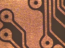
Very fine lines of 30 microns cannot, for obvious reasons, use normal one-ounce copper. As we reduce the line width we must reduce the thickness. At Sierra Circuits, we have manufactured 25-micron lines using 18-micron thick copper but that would be about the upper limit. Thinner copper traces should not be a problem unless your design uses higher current, in which case the specific trace can be made wider to handle the higher current. A 30-micron line is tough and reliable, however, it cannot take a lot of physical abuse which can be nearly eliminated through the use of a typical solder mask.
The fine traces may concern many designers, however, they need to realize the 200-micron wide trace they currently start with reduces down to a 25 to 13-micron aluminum or gold round wire which connects the die to the chip carrier. The fine lines are encapsulated either in the inner layers of the multilayer or by solder mask which means they are virtually locked in. New methods of adhering copper to the circuit board surface have been developed and are used to improve the overall adhesion of a micro trace to the surface. We have a sample board with 40-micron traces without solder mask which we allow customers to scratch at with their fingernails. So far, no one has dislodged a trace.
The first few micro designs had big fillets from the 30-micron trace to the pad. Over time, it has proven unnecessary; routing the trace direct to the pad is very strong and reliable. The extra fillets have just proven to increase image writing time and costs.
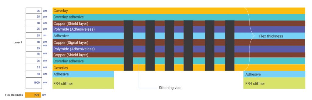
Small vias: there is a physical limit to the size of microvias. Below 50 microns (2 mils) the plating solution will not properly plate the hole wall, resulting in poor via quality. Our laser can drill holes as small as 20 microns, but we can’t plate them. The thickness of the laminate controls the minimum diameter of the vias, with an upper limit of 2:1 for plating micro-vias.
For example, a 3-mil microvia is limited to a six-mil thick laminate with respect to plating. There is also a limit of how deep our Yag laser can drill a via. As the diameter decreases so does the ability to penetrate the laminate for a clean hole. A three-mil via is limited to a four to five mils depth in FR4 and six to seven mils in a glass-free laminate used in HDI applications. All about the microvia is not necessarily bad. The microvia may not be able to be as small as the traces, but we can add a sweetener to the pot since the annular ring around the microvia can be significantly smaller.
The first thing we noticed when we produced our very first micro PCB was that the vias were dead center in the pad. The design used a 9-mil pad and a three-mil via which is tight for conventional printed circuit engineering. The new, more accurate laser manufacturing method would allow as small as a 5-mil pad with a three-mil via, thus saving an enormous amount of board area.
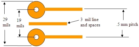
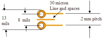
Utilizing new micro circuit design technology instead of the normal printed circuit technology results in significant real estate savings. The best pitch available today with typical 75-micron line widths is approximately .5mm resulting in a 75 micron (3 mils) via with 75-micron lines and a 250 micron (10 mils) pad. The space between the pads is 225 microns (9 mils ) allowing only one 75 micron line between pads and this minimum specification is tough for most shops.
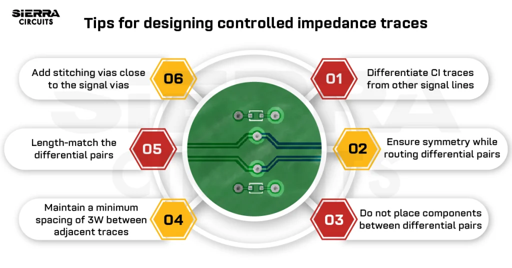
Micro PCB Design Guidelines
Microcircuit technology utilizing a 3-mil via, a 5-mil, a 30-micron line, and 30-micron spaces results in a .2mm pitch layout.
When compared to a standard 3-mil printed circuit board layout, the microcircuit technology results in a five-fold reduction in the area used. In future articles, we will cover ideas to reduce the component area required. However, even with the same components, just switching to 30-micron lines and smaller pads will significantly reduce the board area.
When you route the lines use the same technique but try to angle lines when turning a corner rather than using a single 90-degree turn. The angled lines around the corner spread the corner stress over a wider area.

1. Microvias
When utilizing HDI technology layers added on top of a multilayer board or as an all HDI multilayer, microvias are used to connect between the thin layers. Through-holes can be drilled 5.9 mils in diameter up to 60 mils thick or laser drilled holes 2-3 mils in diameter but only in 2-4 mils thick HDI laminate. Keep in mind that drilled holes wander greatly, compared to laser created holes, which limits the size of the pad to hole. For drilled holes use a 12-mil pad with a 6-mil hole, whereas for a laser-drilled microvia a 5-mil pad can be used with a 3-mil via.
2. Hole Sizes
While it may seem obvious, it’s worth reiterating: every element of a traditional PCB design needs to be adjusted to fit the smaller scale of micro. This can be a challenge for PCB layout engineers familiar with traditional PCB designs. The most common mistake we see in this area is the inclusion of over-sized holes. In fact, micro PCB designs should feature laser microvias to interconnect between substrate layers. If the holes are too large in the design, as is often the case, it will result in suboptimal or even nonfunctioning micro PCBs.
This again goes back to the importance of working with the right micro PCB manufacturer. When the PCB house acts as a partner, you’ll have an expert you can turn to during every step of the PCB process to make sure your micro PCB design meets all necessary requirements.
3. Copper Thickness
Normal 3-mil fine-line circuitry is 1 oz of copper, microcircuits use oz per 30 microns width. Normal pattern plating is used in the manufacture of micro circuits which means the traces do not have to exit the circuit to a plating buss line, pattern plating connects to the entire circuit and wire bonding plating is electroless or electrical.

4. Reliability
Most normal printed circuit laminates can be used for HDI or microcircuits but all have limitations. Micro single and double-sided circuits can be manufactured out of rigid FR4 type laminates however they need to be thin to allow for micro through-holes.
5. Electrical Testing
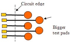
The lower limit of flying probe or even rigid probe (bed of nails) technology is at 2-3 mil pitch right now We expect it to lower over time as necessity requires smaller landing pads. If your micro circuit has smaller points such as edge strip connectors, it is wise to extend the lines off the circuit to a 3-4 mil pad.
6. Solder Mask
The imaging improvements that allow us to manufacture 30-micron lines, unfortunately, has not been transferred to solder mask. 75-micron position accuracy, as well as image resolution, is still the limit.
7. Identification Marking
Typical silkscreen image accuracy is too large for microcircuits. Sierra Proto utilizes a very fine inkjet printer, which results in a significantly small Identification marking resolution.
8. Security Marking
Very small individual bar codes can be imaged into the solder mask to positively identify the printed circuit board. Bar codes can be so small they are virtually invisible to the human eye.
9. Final Finish
Normal printed circuit finishes are available. Most microcircuits use wire bondable soft gold, immersion tin or silver.
10. Know the Manufacturer’s Capabilities
This is by far the most important step to take when working on a micro PCB design, regardless of the specific application or type of microelectronic you want to develop.

This tip is relevant when starting any PCB design work. However, knowing their capabilities and services are especially crucial for micro PCBs. For a company that has never pursued micro PCB designs before or never worked with a given PCB fabrication firm on this type of product, this is essential.
“Micro PCB fabrication capabilities vary greatly from one PCB manufacturer to the next.”
The reason is straightforward: Micro PCB fabrication capabilities vary greatly from one PCB manufacturer to the next. In fact, micro PCBs are still fairly new, and complex enough that many PCB manufacturers will offer limited to no microelectronic capabilities or support. For a micro PCB design to prove successful, you’ll need to ensure the manufacturer is able to meet your base-level requirements.
Keep in mind your design needs to fall within their guidelines. If you incorporate elements into your design which the manufacturer cannot meet, rework will be required. This will lead to delays, slowing both turnaround time and speed to market.
11. Speak to an Engineer
Connect and discuss your next project with an engineer at the PCB manufacturing house early on and, ideally, throughout the design process.
This is especially critical given the fact that, as we’ve covered in previous blog posts, micro PCBs are opening up the realm of microelectronics to countless organizations that have little-to-no experience in this space. For example, a company specializing in blood test equipment may be interested in developing a miniaturized version of this device which requires a miniscule amount of blood for analysis. This is a perfect example of micro PCB’s potential, yet in this case the company in question likely does not have a PCB layout engineer on staff who has worked on micro PCB designs in the past.
This is why it’s crucial to work with a board shop that offers guidance from its own engineers during each step of the micro PCB design process. While some PCB manufacturers, such as Sierra Circuits, deliver this level of service to all of their clients, many do not. If a micro PCB manufacturer does not provide engineer-led support and expertise to clients working on micro PCB designs, then your company should probably look elsewhere early on in the design process.

High-Speed PCB Design Guide
8 Chapters - 115 Pages - 150 Minute ReadWhat's Inside:
- Explanations of signal integrity issues
- Understanding transmission lines and controlled impedance
- Selection process of high-speed PCB materials
- High-speed layout guidelines
Download Now