


Contents

On-demand webinar
How Good is My Shield? An Introduction to Transfer Impedance and Shielding Effectiveness
by Karen Burnham
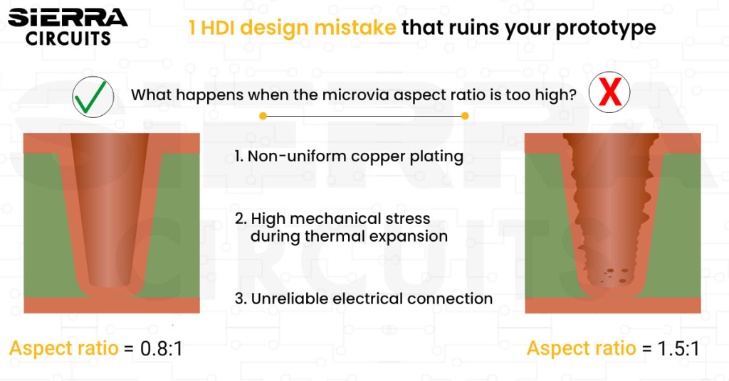
Designing a microvia with an excessive aspect ratio is one of the typical causes of reliability issues in HDI PCBs. It can result in non-uniform plating, increased mechanical stress, and cracks in plated holes.
Fabricators appreciate reviewing the aspect ratio during the design phase, as it allows them to identify manufacturability risks early and recommend changes before they become expensive respins.
For PCB designers, it helps in selecting the right dielectric thickness, via dimensions, and stack-up, reducing design iterations and accelerating time-to-market.
In this article, you’ll learn how aspect ratio affects board reliability, why designers exceed recommended limits, and how to prevent these issues before fabrication.
Highlights:
- Avoid designing microvias with an aspect ratio above 0.8:1, which can make plating less uniform and increase reliability risks.
- Consider both via depth and diameter when designing HDI microvia structures.
- Learn how excessive aspect ratios cause plating defects, thermal stress, and electrical failures.
- Validate your HDI microvia design using a practical fabrication checklist.
Why does microvia aspect ratio matter?
A microvia aspect ratio of 0.8:1 is recommended to achieve reliable copper plating and long-term reliability. This means the hole depth should not exceed 80% of its diameter.
In a recent webinar, how to nail your HDI PCB routing, we asked designers about their biggest challenges in designing microvias. Here’s the result.

29.2% struggle with maintaining adequate drill-to-copper clearance, 27.1% encounter difficulty in selecting the right capture pad diameter, while 43.8% find it challenging to maintain a compatible aspect ratio.
Designers often optimize microvias for routing density without considering what happens during fabrication. A microvia that looks acceptable in the layout can be difficult to drill and plate reliably at the fabrication stage. As the aspect ratio increases, it becomes harder for the plating solution to reach the bottom of the via and deposit uniform copper, increasing the risk of voids, mechanical stress, and cracking.
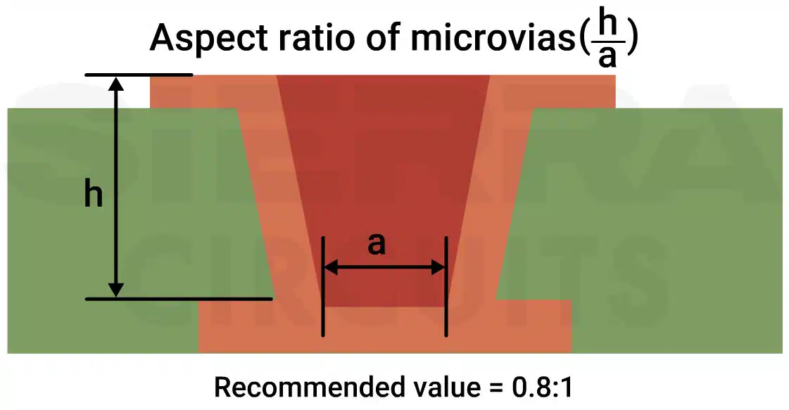
Aspect ratio = via depth ÷ via diameter
As the aspect ratio increases, the via becomes deeper relative to its diameter, making it more difficult to plate.
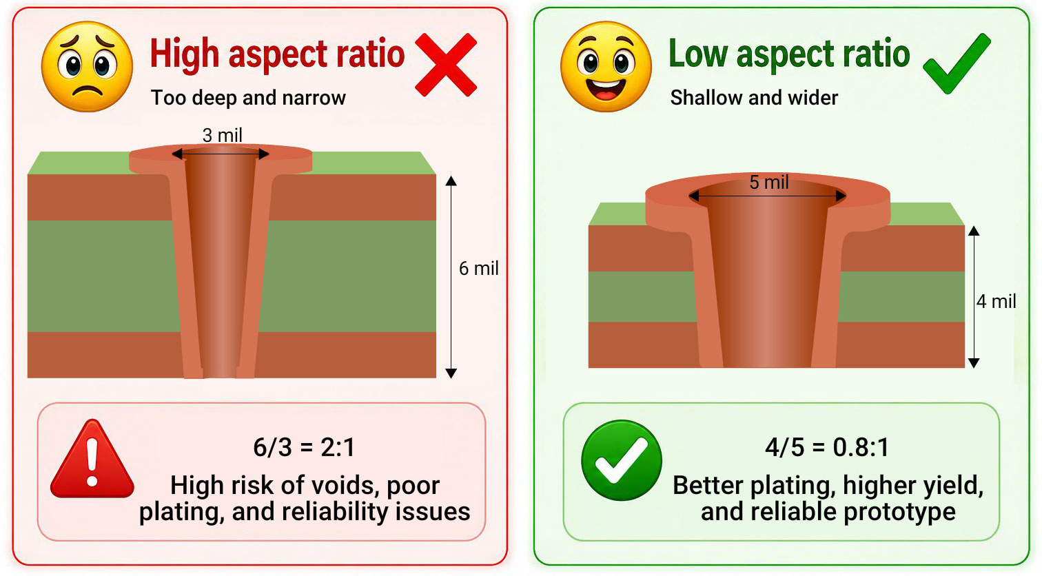
According to IPC-2226 and IPC-T-50, the hole depth should not exceed its diameter, which corresponds to a maximum aspect ratio of 1:1. However, targeting an aspect ratio of 0.8:1 provides a greater process window for laser circuit board drilling and plating, reducing the risk of voids, mechanical stress, and cracking.
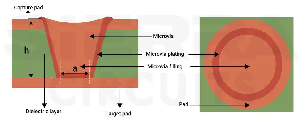
To learn how to build a high-density prototype, download the HDI PCB Design Guide.
HDI PCB Design Guide
10 Chapters - 98 Pages - 90 Minute ReadWhat's Inside:
- Planning your stack-up and microvia structure
- Choosing the right materials
- Signal integrity and controlled impedance in HDI
- Manufacturing considerations for higher yields
Download Now
What design decisions lead to a higher aspect ratio?
Typical causes include increasing the dielectric thickness, reducing the via diameter, and designing without considering the fabricator’s manufacturing capabilities.
1. Increasing the dielectric thickness
The depth of a microvia is determined by the thickness of the dielectric layer it traverses. As the dielectric thickness increases during stack-up development, the aspect ratio increases unless the via diameter is increased accordingly.
2. Reducing the via diameter
HDI designs often use microvias to create additional routing channels between fine-pitch components. Smaller holes improve routing density; they also leave less manufacturing margin for laser drilling and plating.
3. Ignoring fabricator capabilities during stack-up design
Fabricator capabilities, such as lamination, laser drilling accuracy, via filling, and build-up construction, determine the hole dimensions that can be manufactured reliably. Waiting until the design is complete to review these capabilities can result in aspect ratios that exceed the manufacturer’s process limits.
During an interview, Dilip Kumar, Senior Design Manager at Sierra Circuits, explained, “The biggest mistake I see is that designers treat microvias as a routing solution instead of evaluating whether they’re right for the design. Before placing microvias in a stack-up, they should verify that the aspect ratio is within recommended limits, the fabricator can reliably build the structure, the holes can carry the required current, withstand the operating voltage, and provide an effective return path. Overlooking any of these factors can compromise both manufacturability and reliability.”

What happens when the microvia aspect ratio is too high (>0.8:1)?
A high aspect ratio makes copper plating less uniform and increases mechanical stress. Over time, these issues can lead to cracking and intermittent electrical failures.
Let’s look at each of these effects in detail.
1. Microvia separation from the capture pad
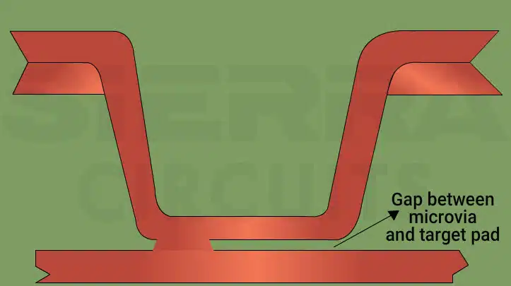
To achieve a reliable interconnection, copper must be deposited uniformly along the hole barrels and at the target pad.
Higher aspect ratios make it more difficult to reach the bottom of the via. This can result in uneven copper deposition, thinner plating at critical places, and a higher risk of defects.
This reduces the mechanical strength of the plated hole and creates weak points that can separate from the capture pad.
According to Steve Carney, R&D Project Manager at Sierra Circuits, “The biggest failure for laser vias is separation between the barrel/fill plating and the capture pad, resulting in opens. This problem was so prevalent that it earned the term “Eyebrowing” because one side of the via remained attached and the separation would form an arc like an eyebrow.”
2. Higher mechanical stress during thermal expansion
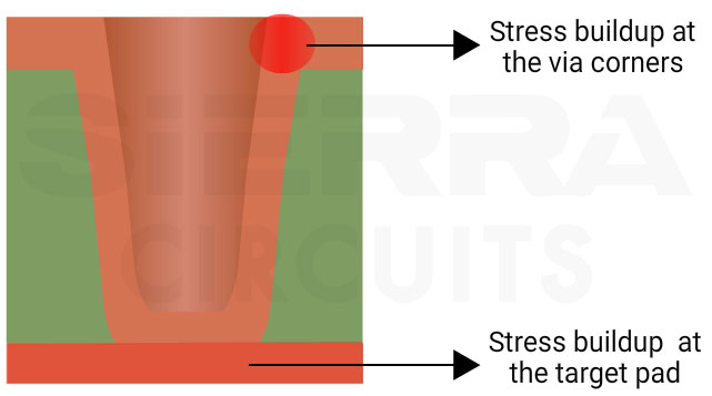
PCBs are exposed to repeated temperature changes during lamination and assembly. As temperatures rise and fall, the dielectric material and copper in the stack-up expand and contract at different rates.
These dimensional changes generate greater mechanical stress within the plated copper. The increased via depth places more strain on the via corners and the interface with the target pad during thermal expansion and contraction.
To validate the reliability of laser-drilled microvias, Sierra Circuits developed its fabrication process using destructive circuit board test coupons that intentionally stressed representative via structures. Early testing revealed separation between the microvia plating and the capture pad in the original design. Based on these results, the capture pad diameter was increased, and the pad surface was optimized to improve the microvia-to-pad interface, eliminating the observed failures.
Every new HDI job begins with a test array and cross-section analysis to verify the microvia geometry and capture pad dimensions. After plating, AOI is performed on the laser-drilled microvias to detect voids and other plating defects before production continues.
3. Unreliable electrical connection
Plating irregularities, voids, and microvia cracks can increase resistance and disrupt current flow through the interconnection. As these defects grow over time, the likelihood of intermittent connections or electrical failures increases.
Need help resolving potential fabrication issues? Book a meeting with our experts, or call us at +1 (800) 763-7503.
How to keep microvia aspect ratios within your fabricator’s capabilities
Finalize the stack-up first before selecting the via diameter, select HDI-compatible materials, and validate the microvia structure during the DFM review. These steps help ensure the geometry aligns with your fabricator’s manufacturing process.
1. Check your fabricator’s microvia capabilities
The fabricator’s drilling, plating, and build-up processes also determine whether the structure can be manufactured reliably.
Before finalizing your microvia dimensions, check your fabricator’s capabilities. Confirm the limits for laser drill diameter, aspect ratio, annular ring, and hole location tolerance.
At Sierra Circuits, our fabrication process supports microvia structures with specific limits for via diameter, aspect ratio, drilling, and plating.
| Laser-via capability | Value |
|---|---|
| Smallest laser drill diameter | 4 mil (0.102 mm) |
| Minimum annular ring, laser drilled | 2 mil (0.051 mm) |
| Laser hole location tolerance | 0.5 mil (0.013 mm) |
| Maximum laser-via aspect ratio | 0.75:1 |
2. Define the build-up before finalizing the via diameter
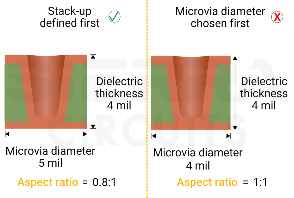
The dielectric thickness between adjacent layers determines the microvia depth. If the hole diameter is selected before the stack-up is finalized, subsequent changes in dielectric thickness can increase the aspect ratio beyond your fabricator’s recommended limit.
For instance, a 5-mil hole initially designed for a 4-mil dielectric has an aspect ratio of 0.8:1. If you later decrease the dielectric thickness to 4 mil without increasing the microvia diameter, the aspect ratio becomes 1:1, reducing the manufacturing margin.
Real-world example:
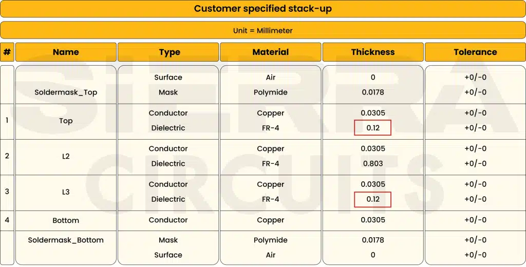
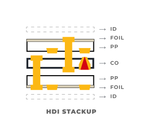
In the stack-up above, the customer-specified dielectric thickness is 0.12 mm (4.72 mil). Including the plating thickness of 0.15 oz (0.20 mil), the total via depth became approximately 4.92 mil.
For laser-drilled vias, the recommended aspect ratio is 0.8:1.
Based on this ratio, the calculated drill diameter was (4.92/0.75) ~6.57 mil.
However, to ensure reliable drilling and plating quality, we recommend limiting laser-drilled via diameters to ≤ 6 mil.
To address this issue, our CAM engineers reduced the dielectric thickness to 4.22 mil (highlighted in green).
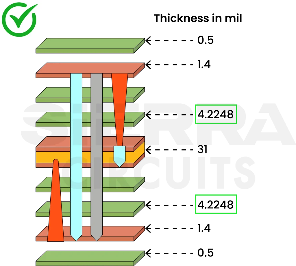
Including the plating thickness of 0.20 mil, the total via depth becomes 4.42 mil.
Applying the recommended laser-via aspect ratio of 0.8:1, the resulting drill diameter is: 4.42/ 0.75 ≈ 5.89 mil, which is less than 6 mil.
Not sure if your HDI stack-up is manufacturable? Schedule a design review with our engineers to validate your microvia structures and avoid potential fabrication issues.

3. Choose HDI-compatible materials and foil construction
The dielectric material and foil construction influence the hole depth and your fabricator’s ability to manufacture the intended HDI stack-up. Selecting unsuitable materials or using a core construction can make it difficult to maintain the recommended microvia aspect ratio.
| Materials | Why it’s used in HDI |
|---|---|
|
Good laser drilling, cost-effective, suitable for most HDI applications. |
|
Low dielectric loss for HDI designs requiring high-speed signal integrity. |

4. Validate the microvia structure during the DFM review
Review the complete microvia structure during the DFM review to confirm it complies with your fabricator’s capabilities.
During an interview, Vadiraj, Senior Manager of Sales Engineering and Business Development of Sales Engineering and Business Development at Sierra Circuits, explained, “Designers generally focus on routing signals through the available space when planning via structures. However, they should also evaluate whether those structures are manufacturable. Otherwise, they may end up with non-manufacturable vias, leading to production delays and stack-up rework.”
We spoke with our experts Dilip Kumar, Senior Design Manager, Steve Carney, R&D Project Manager, and Vadiraj Kulkarni, Senior Manager of Sales Engineering and Business Development at Sierra Circuits, to develop a checklist to ensure reliable microvia fabrication.
| No. | Checklist items | ✓ |
|---|---|---|
| 1 | Finalize the stack-up (dielectric thickness) before deciding the hole dimensions. | ☐ |
| 2 | Keep the aspect ratio at 0.8:1 or lower. | ☐ |
| 3 | Select via dimensions compatible with the dielectric thickness and use staggered holes where possible. | ☐ |
| 4 | Review the microvia structure with your PCB fabricator during the DFM review. | ☐ |
| 5 | Evaluate the hole structures for thermal cycling reliability. | ☐ |
| 6 | Specify all via filling requirements in the fabrication notes. | ☐ |
| 7 | Ensure the annular ring and drill-to-copper clearances meet your PCB fabricator’s capabilities. | ☐ |
| 8 | Maintain a capture pad diameter of at least 80% of the microvia diameter. | ☐ |
Sierra Circuits utilizes self-learning automated scaling software (XACT) to ensure precision in HDI stack-up design. The system analyzes material type, thickness, and copper weight on each layer to accurately predict and compensate for material shrinkage.
Visit HDI PCB capabilities to learn more.
Excessive microvia aspect ratios increase the risk of plating defects, mechanical stress, and long-term reliability failures. By controlling via depth, selecting appropriate diameters, and validating aspect ratios early in the design process, PCB designers can build more reliable HDI interconnects and avoid costly failures later.
About the technical reviewer:
Dilip Kumar is the Senior Design Manager at Sierra Circuits with over a decade of experience in developing high-speed and HDI PCB designs featuring fine-pitch BGAs. He is proficient in Altium Designer, Cadence Allegro, Eagle PCB, KiCAD, and AutoCAD.
Leading a team of skilled PCB designers and layout engineers, he oversees projects from concept to production, ensuring precision and manufacturability at every stage. Dilip consistently delivers innovative, high-quality designs that meet demanding engineering and business objectives.






Start the discussion at sierraconnect.protoexpress.com