Speak to an Account Manager
![]() +1 (800) 763-7503
+1 (800) 763-7503
Related Categories — High Speed » KiCad Tutorials
PCB Material Selection: Electrical and Manufacturing Considerations
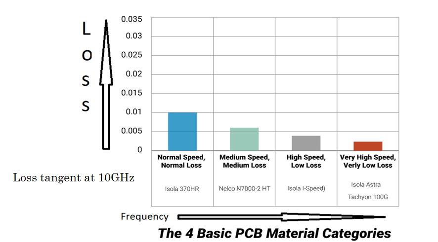
When it comes to PCB material selection, making the right choice for your design is important because materials can impact the overall performance. Knowing how the thermal and electrical properties impact your design before you get to the manufacturing stage can save you time and money while achieving the best results.
PCB Design
How to Reduce Parasitic Capacitance in PCB Layouts
A PCB consists of several parallelly spanned conductors, say traces, separated by an insulator. These traces, along with ... more »
PCB Design
Why We Perform PCB Ionic Contamination Analysis
What can be more problematic than seeing your expensive PCB not performing as intended? What would you do ... more »
PCB Assembly
PCB Material Selection: Electrical and Manufacturing Considerations
When it comes to PCB material selection, making the right choice for your design is important because materials ... more »
PCB Design
How to Reduce Parasitic Capacitance in PCB Layouts
A PCB consists of several parallelly spanned conductors, say traces, separated by an insulator. These traces, along with ... more »
PCB Design
Why We Perform PCB Ionic Contamination Analysis
What can be more problematic than seeing your expensive PCB not performing as intended? What would you do ... more »
PCB Assembly
How to Control your Controlled Impedance
While manufacturing a PCB, controlled impedance can be achieved through specific dielectric thickness and by providing the target ... more »
Controlled Impedance
PCB Drilling Explained: The Dos and the Don’ts
Drilling is the most expensive and time-consuming process in PCB manufacturing. The PCB drilling process must be carefully ... more »
PCB Manufacturing
PCB Manufacturing Defects Caused By Land Patterns
PCB land pattern defects should be treated with due attention since their design is very essential for the ... more »
PCB Assembly
8 Common Errors in Surface Mount Technology (SMT)
Surface mount technology is not a zero-defect soldering process. In this article, we will look into simple defects ... more »
PCB Assembly
How to Achieve a Robust PCB Design Workflow for Signal Integrity?
Signal Integrity (SI) signifies the signal’s ability to propagate along PCB traces without distortion. Signal integrity is about ... more »
PCB Design
How to Choose PCB Laminates and Materials for Fabrication
PCB material selection is the first step in your PCB design process. Selecting the right materials for your ... more »
PCB Design


Fabrication, Procurement, & Assembly. PCBs fully assembled in as fast as 5 days.
- Bundled together in an entirely-online process
- Reviewed and tested by Engineers
- DFA & DFM Checks on every order
- Shipped from Silicon Valley in as fast as 5 days

Fabrication. Procurement & Assembly optional. Flexible and transparent for advanced creators.
- Rigid PCBs, built to IPC-6012 Class 2 Specs
- 2 mil (0.002″) trace / space
- DFM Checks on every order
- 24-hour turn-times available

Complex technology, with a dedicated CAM Engineer. Stack-up assistance included.
- Complex PCB requirements
- Mil-Spec & Class 3 with HDI Features
- Blind & Buried Vias
- Flex & Rigid-Flex boards