Speak to an Account Manager
![]() +1 (800) 763-7503
+1 (800) 763-7503
Related Categories — PCB Assembly » PCB Design
Network Theory for Better PCB Design and Development
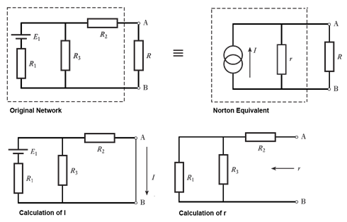
The study of resolving issues with electrical circuits and networks is called network theory. Network theory concepts are essential for network analysis which is critical for the design of PCB transmission lines and power distribution networks. You need to grasp the fundamentals of electrical circuits and network components to master network analysis.
PCB Design
What is a Prepreg in PCB Manufacturing?
As simple as it is, a prepreg is nothing but an insulation layer. Prepreg is a dielectric material ... more »
PCB Design
How to Control your Controlled Impedance
While manufacturing a PCB, controlled impedance can be achieved through specific dielectric thickness and by providing the target ... more »
Controlled Impedance
Network Theory for Better PCB Design and Development
The study of resolving issues with electrical circuits and networks is called network theory. Network theory concepts are ... more »
PCB Design
What is a Prepreg in PCB Manufacturing?
As simple as it is, a prepreg is nothing but an insulation layer. Prepreg is a dielectric material ... more »
PCB Design
How to Control your Controlled Impedance
While manufacturing a PCB, controlled impedance can be achieved through specific dielectric thickness and by providing the target ... more »
Controlled Impedance
Component Placement Guidelines for PCB Design and Assembly
In the era of miniaturization and HDI PCBs, space optimization on the PCB might frequently affect proper component ... more »
PCB Assembly
5 Military Grade PCB Design Rules and Considerations
The term military-grade PCBs can only be used in relation to products manufactured to military specifications. The equipment ... more »
Defense & Space
DDR Memory and the Challenges in PCB Design
Modern electronic designs such as mobiles, laptops, cloud computing, and networking demand very high performance. Apart from processor ... more »
PCB Design
What is Back Drilling in PCB Design and Manufacturing?
There are various challenges when it comes to PCB design and manufacture and one of them is retaining ... more »
PCB Design
Why Are Flex PCBs Used in Medical Devices and Wearables?
Fitness wearables and medical devices have become more popular nowadays. The demand for these devices is expected to ... more »
Flex PCBs
The Advantages of Metal Core Printed Circuit Boards
When the temperature of a PCB assembly starts rising, the owner of that board begins to sweat profusely. ... more »
PCB Design


Fabrication, Procurement, & Assembly. PCBs fully assembled in as fast as 5 days.
- Bundled together in an entirely-online process
- Reviewed and tested by Engineers
- DFA & DFM Checks on every order
- Shipped from Silicon Valley in as fast as 5 days

Fabrication. Procurement & Assembly optional. Flexible and transparent for advanced creators.
- Rigid PCBs, built to IPC-6012 Class 2 Specs
- 2 mil (0.002″) trace / space
- DFM Checks on every order
- 24-hour turn-times available

Complex technology, with a dedicated CAM Engineer. Stack-up assistance included.
- Complex PCB requirements
- Mil-Spec & Class 3 with HDI Features
- Blind & Buried Vias
- Flex & Rigid-Flex boards