Ready to start printing the highest quality basic circuit boards? Our No-Touch service can help you efficiently fabricate your standard bare PCBs, right here in the U.S.
No-Touch PCB
What is No-Touch PCB Service?
Our No-Touch PCB service enables you to get cost-effective bare boards through an online service.
You will have to upload your files and run our automatic DFM file verification before you can place an order.
What does No-Touch Guarantee?
Every No-Touch product comes with the guarantee that if your design has no manufacturability issues and conforms to our guidelines and restrictions, you’ll receive an exemplary board.
Our No-Touch process and manufacturing is highly automated. Your responsibility is to make sure your boards meet our specs and guidelines, and ours is to provide you a board manufactured to that design!
Why is No-Touch different from our other offerings?
With No-Touch PCBs promotion, we always analyze your design files even before you place an order! However, this means that after you upload your design, you need the ability to assign which file is which layer, so that our Automatic File Verification (AFV) program can determine if there are any discrepancies (say, annular ring is not wide enough, or traces are too thin, etc.)
If there are any discrepancies, you will get a detailed report and will have to fix your design and upload again. Once your design passes the AFV, only then can you place an order and your design will be manufactured just like that, with no human intervention (hence “No-Touch”). Because of all the pre-order AFV checks, you can also be sure that your No-Touch order will never go on-hold in the fabrication.
Of course, since No-Touch depends more on automation than CAM engineers, we can provide you with great low prices for your PCBs. On the flip side, you can only order very simple “standard technology” 2 to 6 layer boards with No-Touch.
Design Files
What files must be included to submit an order?
- Gerber files in RS-274X format only (Extended Gerber) or ODB++ format. Do NOT use Gerber X2 format!
AND
- Excellon drill file in ASCII format with the following parameters:
- Units = Inch
- Tool Units = Inch
- Coordinate = Absolute
- Zeros omitted = Trailing
- Number format = 2.4
Common Issues
What are the most common reasons for issues in a No-Touch order?
We have found that if our customers watch out for the following TEN pitfalls in their board design and No-Touch submission, they can be almost 100% sure of getting boards manufactured without issues.
The most Common Issues in a No-Touch order are:
- Corrupt or missing Gerber packages are uploaded.
- Gerber file has not been assigned correctly; as an example, if you assign your bottom copper layer as top layer, accidentally during the AFV submission, you may end up getting bad boards.
- The provided board outline is incomplete. (We need the full outline, not just crop marks.) The board outline must be on one of the layers, preferably on the solder mask layer.
- The layers are not properly aligned in your design.
- The drill file provided is corrupt or incomplete. Also, note that if some of the holes in your design lie outside or on the board outline the job may be rejected. (In No-Touch, we only drill holes INSIDE the board outline.)
- Gerber data is not in 274x format or if the Gerber files are not 1:1 (true size).
- The copper pour areas in your design are filled with trace width of less than 6 mils.
- Actual dimensions of the board do not match those that were entered (we want you to be accurate: eg. 4.35″ X 3.22″).
- More than 1 circuit board design exists on the image. Please include only one circuit board design per order; no multiple part numbers masquerading as one design.
- The design exceeds maximum individual dimension (15.9″) on any side or if a single board area exceeds 100 sq inches.
Design Guidelines
Are there any design tips that can ensure my No-Touch boards are processed smoothly?
Apart from following the overall specs e.g., minimum 0.004″ trace & space,0.005″ minimum annular ring, 0.008″ minimum hole size etc., please follow the following guidelines:
- Provide a full board outline (not just crop marks in the corners). Also ensure that each straight line in the outline is made of one continuous line segment, not multiple line segments.
- Make sure all layers are properly aligned.
- Make sure your drill data is as complete as it can be. And check the design software settings so drill file is output, as follows:
- Format = Excellon
- Data Type = ASCII
- Units = Inch
- Tool Units = Inch
- Coordinate = Absolute
- Zeros omitted = Trailing
- Number format = 2.4
- Make sure all your holes lie within the board outline. Holes on or outside the board outline will not be drilled.
Additionally, after you upload your files, our system will read in your data and ask you to confirm the information. You will be required to provide/confirm the following:
- The polarity (positive or negative) for each of your Gerber files (E.g. whether your plane layer is in positive or negative format).
- Which holes in your drill file are plated and which ones are non-plated.
Data Submission Requirements
What are the data submission requirements?
These data submission requirements will help ensure that your designs easily pass the Auto File Verification.
- Layers must be aligned and viewed from the top side of the board. If your boards are not properly aligned, our auto file verification program will attempt to align them. If it is not able to properly align them, the job may be rejected.
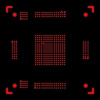
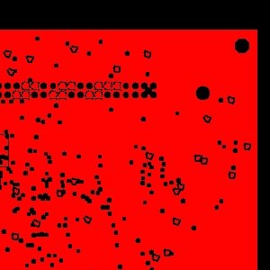
- Crop marks are not allowed.
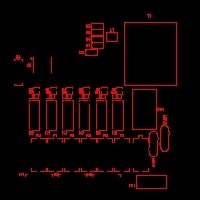
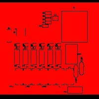
- This figure has crop marks to show the outline. Our automation DOES NOT like this:
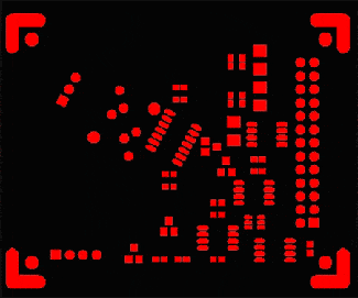
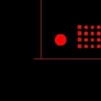
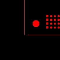
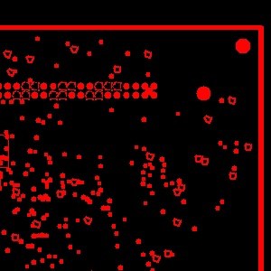
- Correct board outline must be present on one of the board layers (solder mask preferred).The following figure has a proper board outline:
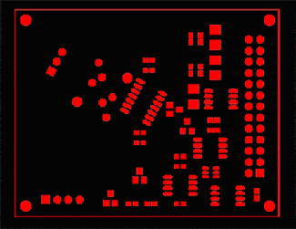
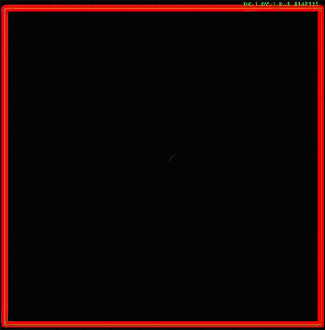
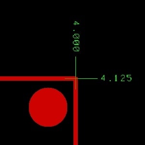
- Please note that the center of the outline needs to be the board outline. The following example is the outline is for a 1×1 inch board, notice that the dimension is being taken from the center of the outline:
Can you show me examples of drill files that are acceptable to your system?
We expect your drill file to be Excellon drill file in ASCII format with the following parameters:
- Units = Inch
- Tool Units = Inch
- Coordinate = Absolute
- Zeros omitted = Trailing
- Number format = 2.4
- Here are two examples of good drill files:
- Example 1:
- R,T
- VER,1
- FMAT,2
- INCH,TZ
- TCST,OFF
- ICI,OFF
- ATC,ON
- T1C0.0350
- T2C0.0550
- T3C0.0650
- T4C0.1300
- %
- M47,OrCAD PCB Drill V2.01
- M47,Holes between Component Layer and Solder Layer
- G05
- T1
- X002595Y000895
- X003057Y000897
- X003860Y003810
- X003905Y004495
- X004395Y007910
- X005500Y019500
- X005500Y030000
- X005650Y005260
- X005920Y004340
- T2
- X013350Y038500
- Example 2:
- %
- T1C0.0350F200S100
- X002595Y000895
- X003057Y000897
- X003860Y003810
- X003905Y004495
- X004395Y007910
- X005500Y019500
- X005500Y030000
- X005650Y005260
- X005920Y004340
- T2C0.0550F200S100
- X013350Y038500
- Example 1:
Board Outlines
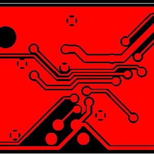
What are the guidelines for board outlines and filled areas?
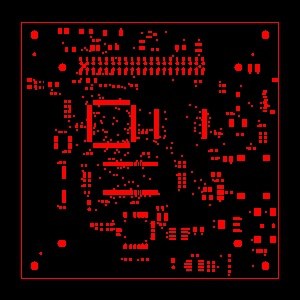
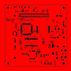
The correct board outline must be provided on one of the Gerber files (we prefer that it be on the solder mask layer). The outline needs to be constructed by a single line (not multiple line segments) that connect to each other (10 mil line width preferred), and the dimensions are calculated using the center of the line.
- Here are examples of good outlines
- Notice how the measurement is taken from the center of the line:
- Crop marks instead of line:
- Here are examples of bad outlines
- Not clean at the corner. Here the outline is made using multiple lines and overlapping lines, instead of a single line. This is not allowed:
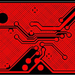
What are some examples of bad outlines with incorrect filled areas?
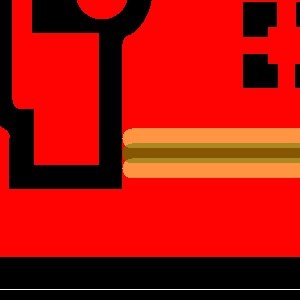
Filled areas must be filled using 10 mil outlines with 1 mil overlap. Use 0 and/or 90-degree lines to do the fill. We have found that some CAD systems will leave gaps in the fill areas when using a 45-degree line. Crosshatch is not allowed. See the following examples:
- This example has a one mil (0.001″) overlap:
- This is an example of a plane area using a Cross Hatch pattern. Cross Hatch patterns are not allowed.
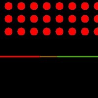
What is necessary to detail regarding positive and negative polarities?
Here are examples that show the requirements in providing direction for positive or negative polarities for different kinds of layers. (Please note: red represents data and black represents the absence of data.)
- Silkscreen:
- Example of positive polarities
- Example of negative polarities
- Solder mask:
- Example of positive polarities
- Example of negative polarities
IMPORTANT NOTE ABOUT solder mask polarity: It is important that you understand that the polarity of solder mask is almost always POSITIVE from a manufacturing perspective. There is some confusion in the industry about this because during the design stage and in many design software these may be referred to as negative, but from a PCB manufacturing perspective, these are called positive.
How can I understand how PCB manufacturers interpret polarity in a solder mask?
If your solder mask data represents the “absence of solder mask” then the data is in POSITIVE polarity. In other words: if your data shows the places which you WANT TO SOLDER, then your solder mask layer is in POSITIVE format.
So when you are in the layer assignment screen on our website, it is most likely that the solder mask should be assigned as positive polarity, as follows:
- Plane layer:
- Example of positive polarities
- Example of negative polarities
- Signal Layer
- Example of negative polarities
- Example of positive polarities

Additional Guidelines
Why does No-Touch recommend a minimum width of 5 mils for silkscreen/legend?
We currently use two different processes to print the silkscreen. One process uses an Ink Jet Printer which uses a 5-mil dot for printing. If your line width is below 5 mils, the line will be printed as 5 mils, but the writing may blotchy and not readable.
The other is a screening process, where a film gets printed on a screen. In this case, if your line width is below 5 mils, it may not get printed at all!
Resolution: If your silkscreen is less than 5 mils, increase the line widths to at least 5 mils and make sure the text is readable after the increase.
Please note that our automated program does not check for the width of silkscreen. It is up to the customer to ensure that the silkscreen width is more than 5 mils. In any case, this requirement does not affect the electrical functionality of the board.
What is automatic sliver repair?
“Slivers” refer to small sections or partials of the dry film. Any small partials of dry film resist have the potential of being lifted off the panel after developing and may re-deposit itself in an area where it could be detrimental to the end product. Such re-deposited resist slivers may cause shorts and/or “opens” on the end product. In a well-designed PCB, features that could result in small dry film resist slivers are modified to increase the amount of resist to aid in the adhesion of the resist to the laminate.
In No-Touch, we have customized our design software to automatically fix slivers in your design. This enables us to provide boards with less chances of shorts and “opens” caused by slivers.


