Try our free Better DFM tool and save time and money.
Our automated platform will catch any PCB design error ahead of time and prevent on-holds and re-spins. Get started by uploading your Gerber files here.
About Better DFM
What is Better DFM?
Better DFM is an online tool to check the Design For Manufacturability. It is run on your PCB design files (Gerber file format) and it gives you detailed information about where it finds design rule issues in your files. For example, if you think your PCB design has a minimum trace of 6 mils, and you run Better DFM, it will highlight any areas where the traces are 5 mils.
How does Better DFM help me?
- Save time and money– Catch your PCB design errors ahead of time and prevent on-holds and re-spins
- Peace of mind– Ensure that you have the complete set of files for manufacturing. Ensure your Gerber files electrically match your CAD design.
- Convenience– Get (optional) instant price quote, place order online.
Why is Better DFM better than other online tools?
Our Better DFM is more flexible and accurate. Along with checking against our core manufacturability rules it also allows you to put in your specific design rules to check against.
You tell us what rules you are designing to and we’ll check against that! For example, in regard to annular rings, you can specify if you want Better DFM to test against tangency or breakout or some specified annular ring minimum width.
We provide a full netlist comparison. If you load your IPC-356 format netlist with your files, we will create a netlist from your Gerber files and compare it with your IPC netlist. If there are any shorts and “opens” we will show you which nets they are on.
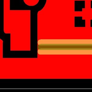
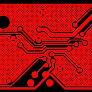
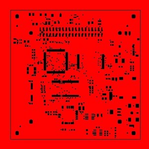
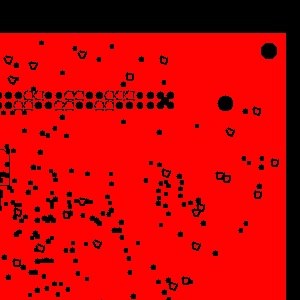
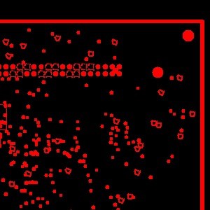
We provide a precise analysis in our DFM, with the exact location and real graphics.
We can accept multiple drill files, and you can indicate which holes are plated or non-plated, and which layers they go through.
Better DFM provides you with a PDF file for each layer, showing how that layer matches up against the drill holes so you can spot any alignment issues.
Our Better DFM is hooked up to our popular Web PCB online service. So (if you choose) you can ask for an INSTANT PRICE QUOTE, and get some of the best value PCB pricing out there. If you choose to order PCBs, it is a cinch. Just pull up your quote and place an order online. It takes less than a minute!
Using the Tool
How do I use Better DFM?
Running Better DFM on your design is an EASY 3-step process:
STEP 1. Log on to our website, put in your design specs and upload your Gerber files.
STEP 2. Our software will unzip your files and present those to you, where you will:
- Identify layer assignment. For each file indicate what layer it is. E.g., sm1.gbr = solder mask top layer, rotator1.gbr = Layer 1, etc.
- Verify drill info and tell us which holes are vias, plated or non-plated.
STEP 3. Get a FREE DFM report in your email. (Including reports for netlist comparison, etc.)
Outputs and Reports
What is the 40-point checklist that Better DFM performs on my PCB design files?
Better DFM does a comprehensive design for manufacturability analysis on your files. Our 40-point checklist includes the following DFM checks:
Signal Checks
- Conductor width
- Spacing
- Annular ring
- Drill-to-copper
- Hole registration
- Text features
- Missing copper
- Features connection
- Missing holes
- Unconnected lines
- Rout to copper
Plane Checks
- Drill-to-copper
- Annular ring
- Spacing
- Conductor width
- Thermal air gap / spoke width
- Missing copper
- Rout to copper
- Drill registration
- Clearance smaller than hole
- Solder mask Checks
Solder mask clearance
- Coverage
- Rout to mask
- Spacing
- Missing solder mask clearance
- Exposed lines
- Partial clearance
- Silk Screen Checks
- Silkscreen to mask spacing
- Silkscreen to copper spacing
- Silkscreen to hole spacing
- Silkscreen to rout spacing
- Line width
- Text height
- Silkscreen over copper text
- Drill Checks
Hole size
- Duplicate holes
- Hole spacing
- Touching holes
- Plane shorts
- Holes to rout
- Missing holes
What do the Better DFM reports look like?
Better DFM provides the following reports:
- REPORT 1. DFM report (provided if we detect any issues in your Gerbers)
- REPORT 2. Netlist report (provided only if we find opens and shorts in your files)
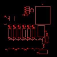
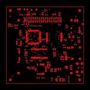
- REPORT 3. PDF images of each layer of your Gerber files
Here are examples of reports:
- DFM report
- Netlist compare report
- Gerber layers shown in PDF format
Common Issues
What are the most common issues I should watch out for before submitting my file for Better DFM?
If you are having trouble running Better DFM, please check for the following most common pitfalls:
- If any file in your Gerber packages is corrupt or missing.
- If some Gerber file has not been assigned correctly; for example, on Layer Assignment screen, if you assign your bottom copper layer as the top layer.
- If a complete board outline has not been provided. (We need a full outline, not just crop marks.) The board outline must be on one of the layers, preferably on the solder mask layer.
- If the layers are not properly aligned in your design.
- If your drill file is corrupt or incomplete.
- If any of your drill holes lie outside or on the board outline OR if your board has NO drill holes!
- If the Gerber data is not in 274x format or if the Gerber files are not 1:1 (true size).
- If the Copper pour areas in your design are filled with trace width of less than 10 mils and less than 1 mil overlap.
- If the actual dimensions of your board are not what you entered. (We want you to be very accurate: e.g., 4.353″ X 3.221″)
- If your netlist file is not in IPC-356 format. (Note that uploading a netlist file is optional.)
Board Outlines and Filled Areas
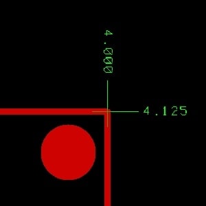
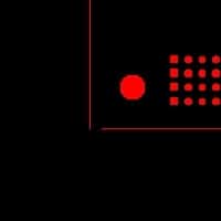
How should I format my board outlines when using the Better DFM Tool?
You need to provide the correct board outline on one of the Gerber files (we prefer it be on the solder mask layer). The outline needs to be constructed by a single line (not multiple line segments) that connect to each other (10 mil line width preferred), and the dimensions are calculated using the center of the line. Please see the following examples for reference:
Examples of a good outline:
(Notice how the measurement is taken from the center of the line.)
Here are some examples of bad outlines:
Crop marks instead of line:
Not clean at the corner:
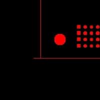
In these examples, the outline is made using multiple lines and overlapping lines instead of a single line. This is not allowed.
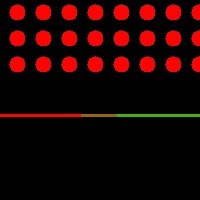
What are the parameters for filled areas within my designs?
Filled areas must be filled using 10 mil outlines with 1 mil overlap. Use 0 and/or 90-degree lines to do the fill. We have found that some CAD systems will leave gaps in the fill areas when using a 45-degree line. Crosshatch is not allowed. Please see the following examples for reference:
- In this example, there is a one mil (0.001″) overlap:
- In the following example, a plane area is using a crosshatch pattern, which are not allowed.
What parameters should be followed regarding positive and negative polarities?
It is important to understand that the polarity of solder mask is almost always POSITIVE from a manufacturing perspective. There is some confusion in the industry about this because during the design stage and in many design software these may be referred to as negative, but from a PCB manufacturing perspective, these are called positive.
Here are examples that will show you what we mean by positive or negative polarities for different kinds of layers. (Please note: red represents data and black represents the absence of data.)
Silkscreen:
Positive
Negative

Solder mask:
Positive
Negative
How can I understand the way that PCB manufacturers interpret polarity in a solder mask?
If your solder mask data represents the “absence of solder mask” then the data is in POSITIVE polarity.
In other words: if your data shows the places which you WANT TO SOLDER, then your solder mask layer is in POSITIVE format.
So when you are in the layer assignment screen on our website, it is most likely that the solder mask should be assigned as positive polarity. Here are some additional examples:
Plane layer
Positive
Negative
Signal layer
Positive

Negative

Annular Ring Width Checks
What are different types of options that Better DFM provides for minimum annular ring width checks?
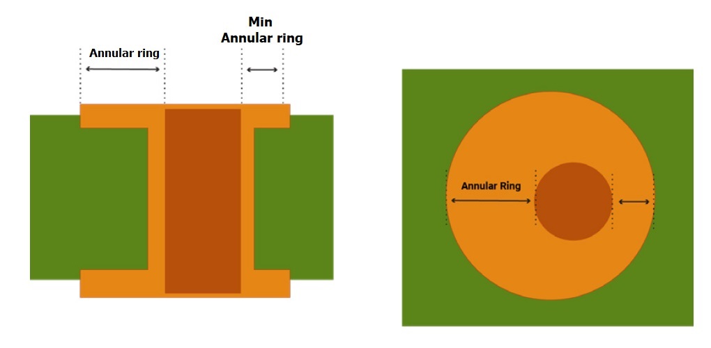
The annular ring width refers to the width of the pad surrounding the hole.
Let’s clarify by using an example. If the pad is 20 mils diameter and hole is 8 mils diameter, then the annular ring width is (20 – 8)/2 = 6 mils. See more details about annular rings.
When you run Better DFM, you can go under “Advanced Options” and choose should be checked about your annular rings.
You have four options to choose from:
- If you are okay with accepting tangency on pads in the manufactured board, then our DFM will look for a minimum of 5 mils (0.005″) annular ring width in your design. (Tangency is the default option, and the DFM will check for 5 mils minimum annular ring width.)
- For those who wish to have a minimum 1 mils annular ring on pads in the manufactured board, then our DFM will look for a minimum of 6 mils (0.006″) annular ring width in your design.
- For a minimum 2 mils annular ring on pads in the manufactured board, then our DFM will look for a minimum of 7 mils (0.007″) annular ring width in your design.
- In the event that you are okay with accepting breakouts on pads in the manufactured board, then our DFM will NOT look for any minimum annular ring width in your design. (NOTE: accepting breakouts is typically NOT recommended!)
Plating Types
When I assign the “plating type” to holes during the Better DFM process, what do the different options mean?
When you are on the second screen of Better DFM we show you all the different drill hole sizes you have in your Gerbers and ask you to assign a “plating type” to each hole size.
Please use this guide to assign:
- PLT = Plated through hole
- Via = Via hole (which is also plated). Properly setting via holes eliminates “missing PTH clearance” issues when via holes are covered with mask.
- NPT = Non-plated through hole
- Laser = Laser hole (which is also plated)
I have intentionally covered my via holes with a mask. But I get a “missing PTH clearance” problem. How can I eliminate this?
During the submission process, there is a page called the drill Information. You need to set the plating type to via for these holes. This will let the system know that the holes are used only for vias and being covered with a mask is OK.
Additional Tips and Support
Are there any additional tips for running Better DFM?
If your design has holes (of a certain size) that are tented with solder mask, you can assign them as vias on the drill Information screen of Better DFM. That way Better DFM will not flag them as being covered with a solder mask.
If your design files have a separate file for the board outline layer, assign that as “Drawing/Other” in the Layer Assignment screen.
Who do I contact for support?
If you have any issues or questions about Better DFM:
- Send us an email at BetterDFM@protoexpress.com
- Contact us by phone at 800-763-7503 and ask for “Better DFM Support team”
- Submit an online service request.


