


Contents
Measuring ultra-low impedances (20 micro-ohms) is a challenge for any power distribution network (PDN) design engineer. The 2-port shunt-through measurement is the standard method for measuring milliohm impedances up to very high frequencies (GHz). Unfortunately, this measurement includes an undesirable ground loop related to the instrument grounds and test setup cabling. The ground loop introduces significant errors if proper care is not taken. This application note shows how to measure as low as 20 μΩ using the Picotest J2102A as a ground loop breaker.
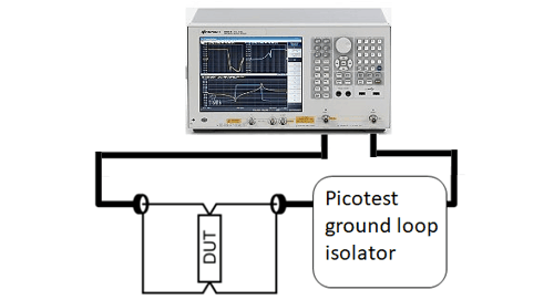
Figure 1 shows the measurement set up to measure impedance in 2-port shunt-through configuration using the Keysight E5061B vector network analyzer (VNA) and Picotest ground isolators – either J2102A or J2113A. Picotest solutions work with any commercial VNA, oscilloscope, or spectrum analyzer. The J2102A (common mode transformer) is used to measure impedances at and above 20 μΩ. J2113A (semi-floating differential amplifier) can be used to measure impedances at or above 1 mΩ. The J2113A is effective down to DC, while the J2102A is effective at, or even below, 100 Hz. This application note describes the measurement at or above 20 μΩ, and the measurements use J2102A which are effective at or above 100 Hz.
Basic theory of the 2-port shunt-through measurement
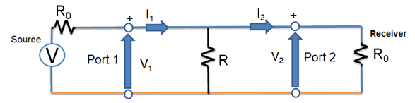
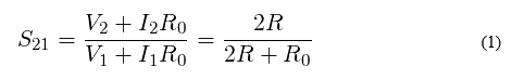
Figure 2 shows the circuit configuration to measure a small valued resistor in 2-port shunt-through measurement. From the definition of S21 [1, pp. 2-3],
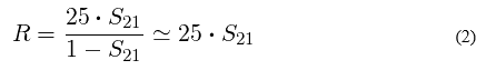
Solving for R we get,
where it is assumed that R0 = 50 Ω and S21 << 1 (True for very small impedance magnitudes/resistances – R << R0). Equation 1 is less intuitive in 2-port shunt-through measurements. Another representation of the definition of S21 is shown in [1, pp. 2],
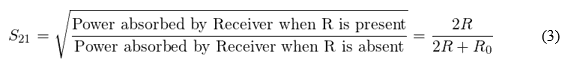
After simplification, Equation 3 results in the same value for S21. The difference here is that Equation 3 gives an intuitive feeling for what is happening with S21 compared to Equation 1. The denominator (= Power absorbed by Receiver when R is absent) is constant for a VNA, if the source and receiver impedances are fixed. One exception to this is proposed by Steve Sandler in his paper “Extending the usable range of the 2-port shunt-through impedance measurement” [2]. Here the source R0 is increased to shift the measurement window. The source and receiver R0 are increased to a higher value by adding an external resistor say, 450 Ω. The Rs now becomes 500 Ω for a 50 Ω VNA assuming that the frequency range we are interested in is such that the external resistor is electrically very small and is a lumped element at that frequency. This method effectively reduced the maximum power that can be sourced from a VNA, which increases the range of impedances that can be measured. It should be noted that the sensitivity is an inherent property of a VNA, and is not changed here.
This means that the minimum measurable value and maximum measurable value are both increased.
In Equation 3, S212 is the received power in Rx scaled by the power that could have been received if the DUT was not present. Let us look at the effect of this in 2-port impedance measurements. R = 25 ⋅ S21, and S21 increases when the received power increases.
Any increase in the received power will be reflected or sensed by the VNA measurement system as an increase in the DUT resistance, R. This is important in understanding the ground loop problem.

Non-idealities and the Inherent Ground Loop
Like all other measurements, the 2-port shunt-through measurements also suffer from non-idealities. Figure 3 shows two non-idealities,
- Cable losses
- Ground loop
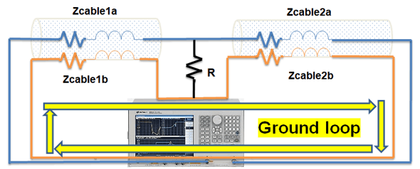
Every cable will have cable losses which are marked as cable resistances in Figure 3. Due to National Electrical Code (NEC) requirements for public safety, all grounds in a VNA have to be connected together. This forms a ground loop in the 2-port shunt-through measurements as shown in Figure 3.
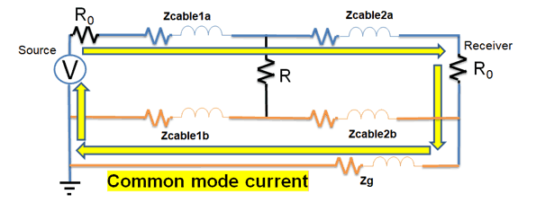
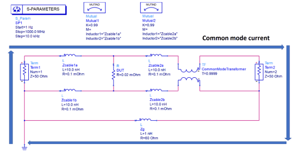
Figure 4 shows an alternate path for signal current return, referred to as common mode current. The addition of ground connections created this path. If this path never existed, all the current would have returned through the cable. The new path created an additional path for current which depends upon the value of Zg. In almost all VNAs, Zg << Zcable1b and Zcable2b. So the additional current is much larger compared to the case of not having this additional path. This additional current adds more power in the Receiver which causes to increase S21 and in turn the estimated R which 25 ⋅ S21. This is an error in measurements, and does not relate to the actual value of R.
Also read: The Pros and Cons of Composite Amplifiers
Solutions to ground loop problem
The common mode current should be minimized to minimize the measurement error. Picotest offers two solutions to minimize common mode current:
- Common mode transformer – J2102A
- Semi-floating differential amplifier – J2113A
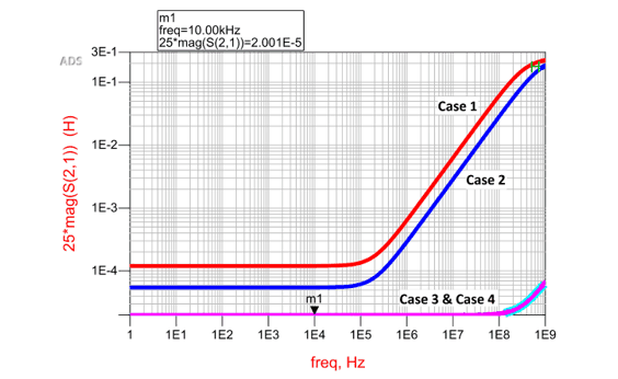
The J2113A can be used at and above DC frequencies, and at voltages from -1.9V to +1.9V, while the J2102A is effective at and above 100 Hz. At frequencies above a few kHz, the common mode rejection ratio (CMRR) of the J2102A is significantly higher than that of the J2113A. In most cases, the J2102A is a better choice for measuring ultra-low impedance (20 μΩ). The J2113A can be used to measure impedance at and above 1 mΩ and at frequencies down to DC. Figure 5 shows Keysight ADS simulations for four cases,
- Ground impdance, Zg = 1 nH + 0.1 mΩ, Common mode transformer, T = 0
- Ground impdance, Zg = 1 nH + 60 Ω, Common mode transformer, T = 0
- Ground impdance, Zg = 1 nH + 0.1 mΩ, Common mode transformer, T = 0.9999
- Ground impdance, Zg = 1 nH + 60 Ω, Common mode transformer, T = 0.9999
The simulation results are shown in Figure 6. E5061B has an inbuilt ground isolation amplifier that mimics of 60 Ω (30 Ω per port) [3, Figure 21] to improve the CMRR of the VNA. Figure 6 shows that this is not good enough when we measure ultra-low impedance (20 μΩ). Cases 3 and 4 shows that when a high-quality common mode transformer is present, good results can be achieved for measurements as low as 20 μΩ.
Making Connections
High fidelity measurement requires high-quality cables and probes, with high shielding effectiveness. Sometimes it is also important to AC couple the measurement in order to minimize DC loading or due to the operating voltage of the measurement exceeding the limits of the VNA. The Picotest PCK01 is a high-performance cable and connector kit while the Picotest P21B01 includes high-quality probes and DC Blocks. The highest accuracy when measuring bulk and decoupling capacitors is achieved by mounting the component on a characterized printed circuit board. The Picotest DTBK01 kit includes most standard sizes and includes de-embedding data to remove parasitics of the PCB from the measurement.
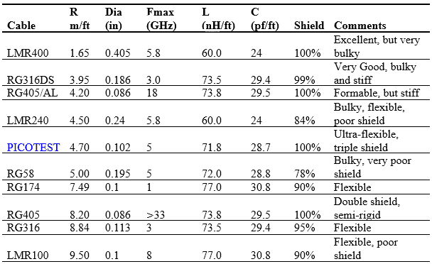
Table 1 shows a comparison of various cable characteristics. Picotest cables provide the best compromise for ultra-low impedance measurements in terms of loss, flexibility, and shielding characteristics. Picotest cables are made especially for accurate, 2-port impedance measurement.
Measurement Examples

Controlled Impedance Design Guide
6 Chapters - 56 Pages - 60 Minute ReadWhat's Inside:
- Understanding why controlled impedance is necessary
- Stack-up design guidelines
- How to design for impedance
- Common mistakes to avoid
Download Now
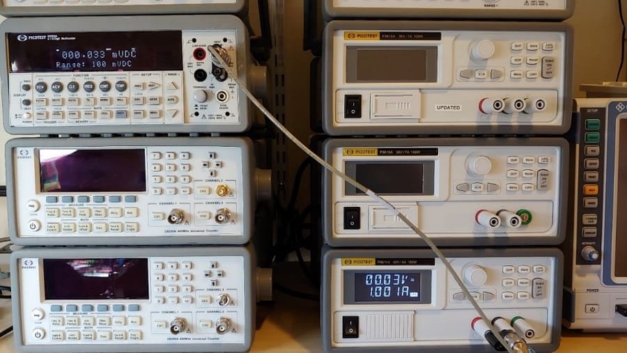
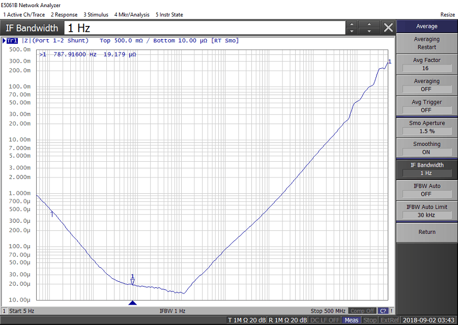
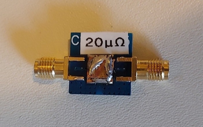
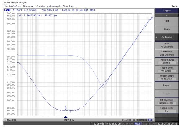
Figure 7 shows the comparison of the measured impedance with and without the Picotest ground loop isolator J2102A while measuring an 88 μΩ resistance. Figure 8 shows the 20 μΩ sample mounted on a fixture for measurements. All the measurements in this article use similar custom made samples mounted on similar fixtures. Figure 9 shows the sample verification at DC by employing 4 wire Kelvin measurement for the 33 μΩ sample.
Figure 10 shows the experimental results of the measured 20 μΩ sample. Cable losses and CMRR of the ground loop breaker are important sources of error in this ultra-low impedance measurement [5]. High-quality cables and Picotest J2102A having very high CMRR are used in these measurements to overcome the errors.
Conclusion
This application note studied the fundamental reason behind the existence of inherent ground loop in a 2-port shunt-through impedance measurement system. Common mode current flowing through the measurement system introduces an error in the received signal in the VNA, and is erroneously sensed as an increase in the resistance of the DUT. The Picotest J2102A or J2113A products eliminate the ground loop in any commercial VNA used to measure impedance in the 2-port shunt-through configuration. J2113A is effective in isolating grounds when we are measuring impedances at and above 1 mΩ. J2113A can be used to isolate grounds at and above DC whereas J2102A can be used to isolate grounds at and above 100 Hz. J2102A can be used to measure impedances at and above 20 μΩ. In this article, the measurement result is presented for 20 μΩ.
Measuring ultra-low impedance requires high-quality cables, and the Picotest cables are made specifically for these applications. It is important to start with a known value of resistance in any measurements to validate the setup. In this application note, a 4 wire Kelvin measurement is used to verify the measurement sample at DC.
Similar ground loops are present in other instruments and test setups, and the Picotest ground isolators are effective there as well. For additional information and products please visit
https://www.picotest.com/measurements/2-portUltralowImpedance.html
References
[1] R. W. Anderson, “S-parameter techniques for Faster, More Accurate Network Design,” HP Appl. note 95-1, Feb. 1967.
[2] S. M. Sandler, “Extending the usable range of the 2-port shunt through impedance measurement,” IEEE MTT-S Lat. Am. Microw. Conf. (LAMC), pp. 1–3, Dec 2016.
[3] “Measuring Frequency Response with the Keysight E5061B LF-RF Network Analyzer,” Keysight Technol. Appl. note.
[4] P. Carrier, “Signal integrity and power integrity in highspeed design,” EDN, 2014.
[5] S. M. Sandler, “How to measure ultra-low impedance (100uOhm and lower) PDNs,” EDICON, Oct. 2018.
For more design information, contact our DESIGN SERVICE team. and visit our controlled impedance capabilities page.
Controlled Impedance Design Guide
6 Chapters - 56 Pages - 60 Minute ReadWhat's Inside:
- Understanding why controlled impedance is necessary
- Stack-up design guidelines
- How to design for impedance
- Common mistakes to avoid
Download Now


