Speak to an Account Manager
![]() +1 (800) 763-7503
+1 (800) 763-7503
Related Categories — HDI / Blind & Buried Vias » High Speed » PCB Design » PCB Experts
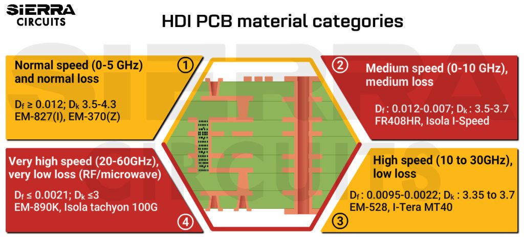
How to Choose the Right HDI PCB Materials
Choosing the right dielectric material for a PCB is important no matter what application you’re working. However, the stakes are higher with high-density interconnect (HDI) technologies.
HDI / Blind & Buried Vias
Top 5 HDI PCB Routing Challenges and Ways to Mitigate Them
HDI designs pose complex routing challenges due to their tight spacing between components and traces. Using DRC settings in ... more »
HDI / Blind & Buried Vias
How to Design Reliable Microvias in Your PCBs
Microvia failure occurs due to the thermal stresses that arise during the PCB assembly process. These stresses can ... more »
HDI / Blind & Buried Vias
How to Choose the Right HDI PCB Materials
Choosing the right dielectric material for a PCB is important no matter what application you’re working. However, the ... more »
HDI / Blind & Buried Vias
Top 5 HDI PCB Routing Challenges and Ways to Mitigate Them
HDI designs pose complex routing challenges due to their tight spacing between components and traces. Using DRC settings in ... more »
HDI / Blind & Buried Vias
How to Design Reliable Microvias in Your PCBs
Microvia failure occurs due to the thermal stresses that arise during the PCB assembly process. These stresses can ... more »
HDI / Blind & Buried Vias
High-Speed and HDI PCB Design Strategies by Syed Ubaid Ali Warsi
Syed Ubaid Ali Warsi, the owner of Wavetroniks, provided his insights into high-speed and HDI PCB design strategies ... more »
HDI / Blind & Buried Vias
10 HDI PCB Design Tips to Maintain Signal Integrity
When it comes to designing HDI PCBs, a plethora of challenges await, including complex routing requirements, issues related ... more »
HDI / Blind & Buried Vias
Case Study: Designing 8 and 14-Layer HDI PCBs with Stacked Vias
Stacked vias are considered the most suitable solution for manufacturing HDI boards with advanced features. The configuration, with ... more »
Case Studies
How Sequential Lamination is Performed to Manufacture HDI PCBs
Sequential lamination is a process of fabricating a circuit board using subsets composed of copper and dielectric layers. ... more »
HDI / Blind & Buried Vias
Case Study: Designing an HDI Board with 0.4 and 0.65 mm BGAs
BGA technology makes it possible to achieve a smaller form factor in PCBs. With a higher pin count, ... more »
Case Studies
How System-in-Package (SiP) Facilitates HDI PCB Designs
We ran into Vern Solberg of Solberg Technical Consulting at PCB West 2022 and discussed the features of ... more »
HDI / Blind & Buried Vias


Fabrication, Procurement, & Assembly. PCBs fully assembled in as fast as 5 days.
- Bundled together in an entirely-online process
- Reviewed and tested by Engineers
- DFA & DFM Checks on every order
- Shipped from Silicon Valley in as fast as 5 days

Fabrication. Procurement & Assembly optional. Flexible and transparent for advanced creators.
- Rigid PCBs, built to IPC-6012 Class 2 Specs
- 2 mil (0.002″) trace / space
- DFM Checks on every order
- 24-hour turn-times available

Complex technology, with a dedicated CAM Engineer. Stack-up assistance included.
- Complex PCB requirements
- Mil-Spec & Class 3 with HDI Features
- Blind & Buried Vias
- Flex & Rigid-Flex boards