Speak to an Account Manager
![]() +1 (800) 763-7503
+1 (800) 763-7503
Related Categories — PCB Manufacturing » PCB Materials
How to Choose PCB Laminates Based on IPC Standards
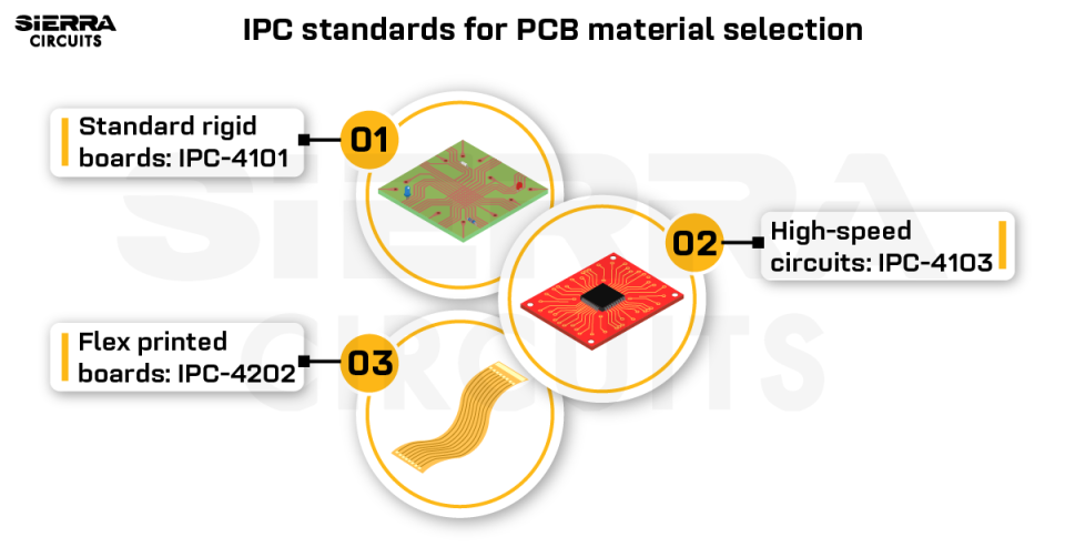
Following IPC standards for PCB laminates makes it easier to choose dielectric materials that fit the specific needs of rigid, […]
IPC
Designing and Fabricating Ultra-HDI PCBs
Ultra-HDI PCBs are becoming essential in high-speed applications such as AI systems, where circuit density and signal integrity ... more »
HDI / Blind & Buried Vias
What is ITAR, the International Traffic in Arms Regulations?
Think about the technology that your company has developed recently and planning to have a patent. You are ... more »
Defense & Space
How to Choose PCB Laminates Based on IPC Standards
Following IPC standards for PCB laminates makes it easier to choose dielectric materials that fit the specific needs ... more »
IPC
Designing and Fabricating Ultra-HDI PCBs
Ultra-HDI PCBs are becoming essential in high-speed applications such as AI systems, where circuit density and signal integrity ... more »
HDI / Blind & Buried Vias
What is ITAR, the International Traffic in Arms Regulations?
Think about the technology that your company has developed recently and planning to have a patent. You are ... more »
Defense & Space
PCB Stack-Up: Plan, Design, Manufacture and Repeat
Often ignored, it is important to understand the difference between an HDI stack-up and a standard stack-up. The ... more »
PCB Design
5 DFM Issues Designers Should Check Before PCB Manufacturing
Every PCB should be designed in such a way that the overall cost and chances of potential DFM ... more »
PCB Design
How to Choose the Right PCBs for IC Integration
Selecting the right PCBs for IC integration depends on the chip’s signal characteristics, power demands, and the end ... more »
PCB Assembly
IPC Class 2 VS Class 3: The Different Design Rules
As circuit board manufacturers, designers often ask us about the difference between IPC Class 2 and Class 3. ... more »
IPC
Why Controlled Impedance Really Matters
Every day, PCB designs and components become smaller, faster – in other words, more complicated. It is now ... more »
Controlled Impedance
A Complete Guide to PCB Interfaces and Communication Protocols
The choice of the PCB interface plays a critical role in enabling efficient protocol layering, minimizing crosstalk, and ... more »
High Speed


Fabrication, Procurement, & Assembly. PCBs fully assembled in as fast as 5 days.
- Bundled together in an entirely-online process
- Reviewed and tested by Engineers
- DFA & DFM Checks on every order
- Shipped from Silicon Valley in as fast as 5 days

Fabrication. Procurement & Assembly optional. Flexible and transparent for advanced creators.
- Rigid PCBs, built to IPC-6012 Class 2 Specs
- 2 mil (0.002″) trace / space
- DFM Checks on every order
- 24-hour turn-times available

Complex technology, with a dedicated CAM Engineer. Stack-up assistance included.
- Complex PCB requirements
- Mil-Spec & Class 3 with HDI Features
- Blind & Buried Vias
- Flex & Rigid-Flex boards