Speak to an Account Manager
![]() +1 (800) 763-7503
+1 (800) 763-7503
Related Categories — Flex PCBs » PCB Design » PCB Materials
Designing and Fabricating Ultra-HDI PCBs
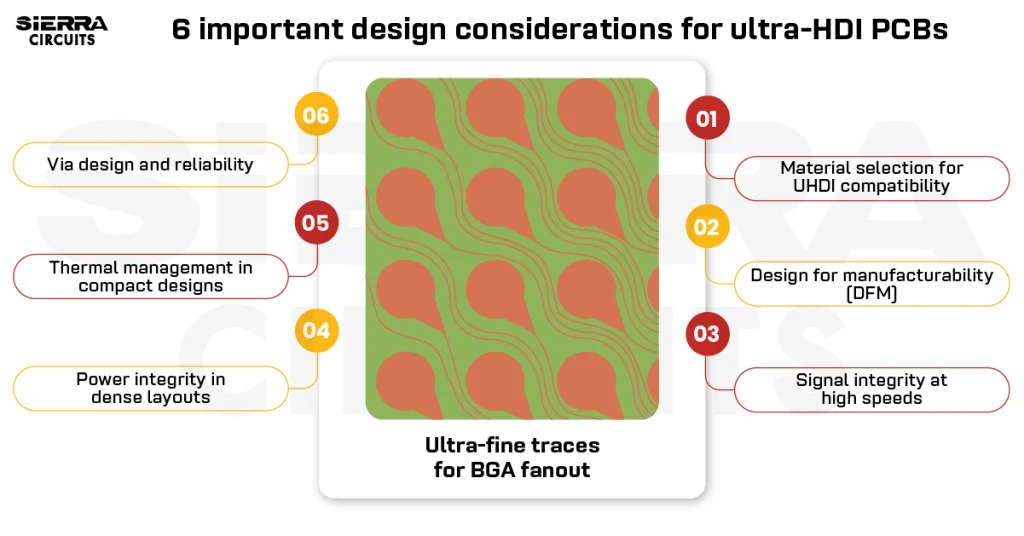
Ultra-HDI PCBs are becoming essential in high-speed applications such as AI systems, where circuit density and signal integrity are critical. […]
HDI / Blind & Buried Vias
What is ITAR, the International Traffic in Arms Regulations?
Think about the technology that your company has developed recently and planning to have a patent. You are ... more »
Defense & Space
5 DFM Issues Designers Should Check Before PCB Manufacturing
Every PCB should be designed in such a way that the overall cost and chances of potential DFM ... more »
PCB Design
Designing and Fabricating Ultra-HDI PCBs
Ultra-HDI PCBs are becoming essential in high-speed applications such as AI systems, where circuit density and signal integrity ... more »
HDI / Blind & Buried Vias
What is ITAR, the International Traffic in Arms Regulations?
Think about the technology that your company has developed recently and planning to have a patent. You are ... more »
Defense & Space
5 DFM Issues Designers Should Check Before PCB Manufacturing
Every PCB should be designed in such a way that the overall cost and chances of potential DFM ... more »
PCB Design
Why Controlled Impedance Really Matters
Every day, PCB designs and components become smaller, faster – in other words, more complicated. It is now ... more »
Controlled Impedance
Humanoid Robotics PCB Design and Advanced Manufacturing Techniques
Humanoid robotics PCBs enable communication between sensors, actuators, and AI processors, a critical factor in building advanced robots. ... more »
PCB Design
How to Design a PCB with Embedded Components
Embedded PCB components are passive devices fabricated within the PCB substrate using conductive and dielectric materials. This integration ... more »
PCB Assembly
Annular Ring Explained by a PCB Manufacturer
Annular rings are one of the biggest concerns of PCB designers. You know that you may place your ... more »
PCB Design
Microwave PCB Material Selection and CPW for Signal Integrity
Designing microwave boards involves meticulous selection of PCB materials, precise etching, and careful management of electromagnetic effects. These ... more »
PCB Design
Try the KiCad Plugin for an Instant PCB Quote
Get instant PCB fab and assembly cost estimation for your designs through Sierra Circuits’ KiCad quote plugin. You ... more »
KiCad Tutorials


Fabrication, Procurement, & Assembly. PCBs fully assembled in as fast as 5 days.
- Bundled together in an entirely-online process
- Reviewed and tested by Engineers
- DFA & DFM Checks on every order
- Shipped from Silicon Valley in as fast as 5 days

Fabrication. Procurement & Assembly optional. Flexible and transparent for advanced creators.
- Rigid PCBs, built to IPC-6012 Class 2 Specs
- 2 mil (0.002″) trace / space
- DFM Checks on every order
- 24-hour turn-times available

Complex technology, with a dedicated CAM Engineer. Stack-up assistance included.
- Complex PCB requirements
- Mil-Spec & Class 3 with HDI Features
- Blind & Buried Vias
- Flex & Rigid-Flex boards