Speak to an Account Manager
![]() +1 (800) 763-7503
+1 (800) 763-7503
Related Categories — PCB Manufacturing
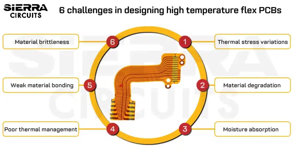
Designing High-Temperature Flex PCBs: 6 Challenges with Solutions
Designing flex PCBs for high-temperature (>125°C) applications presents challenges like thermal stress and trace delamination. You can overcome these issues […]
Flex PCBs
How to Design a PCB with Embedded Components
Embedded PCB components are passive devices fabricated within the PCB substrate using conductive and dielectric materials. This integration ... more »
PCB Assembly
What is Thermal Profiling in PCB Assembly?
In the production and assembly of electronic products, precise control of process parameters is essential. This is done ... more »
PCB Assembly
Designing High-Temperature Flex PCBs: 6 Challenges with Solutions
Designing flex PCBs for high-temperature (>125°C) applications presents challenges like thermal stress and trace delamination. You can overcome ... more »
Flex PCBs
How to Design a PCB with Embedded Components
Embedded PCB components are passive devices fabricated within the PCB substrate using conductive and dielectric materials. This integration ... more »
PCB Assembly
What is Thermal Profiling in PCB Assembly?
In the production and assembly of electronic products, precise control of process parameters is essential. This is done ... more »
PCB Assembly
Annular Ring Explained by a PCB Manufacturer
Annular rings are one of the biggest concerns of PCB designers. You know that you may place your ... more »
PCB Design
Microwave PCB Material Selection and CPW for Signal Integrity
Designing microwave boards involves meticulous selection of PCB materials, precise etching, and careful management of electromagnetic effects. These ... more »
PCB Design
Try the KiCad Plugin for an Instant PCB Quote
Get instant PCB fab and assembly cost estimation for your designs through Sierra Circuits’ KiCad quote plugin. You ... more »
KiCad Tutorials
How to Pick RF PCB Materials: 7 Important Factors to Consider
When designing RF PCBs, selecting the right material is pivotal for achieving optimal board performance. The properties of ... more »
High Speed
Case Study: Reverse Engineering a Flex PCB to Generate Design Files
Our PCB design engineers reverse-engineered a flex circuit to recreate the design files and optimize the LCD connectivity. ... more »
Case Studies
How to Reduce Your PCB Assembly Cost
Maintaining the highest quality standards in boards while simultaneously reducing PCB assembly costs can be an ongoing struggle ... more »
PCB Assembly


Fabrication, Procurement, & Assembly. PCBs fully assembled in as fast as 5 days.
- Bundled together in an entirely-online process
- Reviewed and tested by Engineers
- DFA & DFM Checks on every order
- Shipped from Silicon Valley in as fast as 5 days

Fabrication. Procurement & Assembly optional. Flexible and transparent for advanced creators.
- Rigid PCBs, built to IPC-6012 Class 2 Specs
- 2 mil (0.002″) trace / space
- DFM Checks on every order
- 24-hour turn-times available

Complex technology, with a dedicated CAM Engineer. Stack-up assistance included.
- Complex PCB requirements
- Mil-Spec & Class 3 with HDI Features
- Blind & Buried Vias
- Flex & Rigid-Flex boards