Speak to an Account Manager
![]() +1 (800) 763-7503
+1 (800) 763-7503
Tools for Designers:
PCB Material Selector
Get Started NowPCB material selection is the first step in your design process. Selecting the dielectric material for your design is very important, as it can impact the overall performance of the board. To help board designers determine what sort of material best suits their design needs, we have developed a circuit board material selector.
Sierra Circuits’ PCB Material Selector allows you to search and compare the properties and specifications of board materials that fit your application. There are 50+ rigid materials and 10+ flex materials available in this tool. For each material, there are various parameters listed, such as dielectric constant, dissipation factor, glass transition temperature, decomposition temperature, moisture absorption, etc.
Features of our material selector tool:
- Can quickly find the materials (rigid or flex) suitable for your application
- Provides a datasheet for any given material instantaneously
- Allows you to compare materials that fit your application criteria, such as IPC revisions, slash numbers, Tg, Dk, and lead-free compatibility
How to select the best PCB material
Our circuit board material tool allows you to search and compare PCB materials that fit your application and meet your requirements.
All the criteria for comparative selection are listed below:
Initial selection criteria
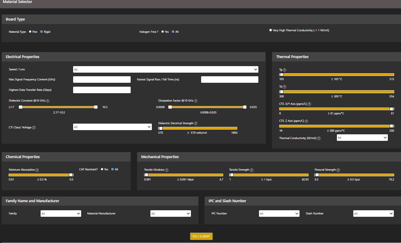
In the Board Properties section, you can choose the following options:
-
- Material type (flex or rigid)
- Halogen-free (yes or all)
- Very high thermal conductivity
Material type: Rigid
If you select rigid as the material type and click on the “Go/Submit” button, our Material Selector lists out all the available rigid materials (even if no criteria are selected).
After selecting the required criteria, click on the “View” button to view the properties of that particular material. To compare the properties, select two or more different materials and hit the “Compare” button. A new window pops up comparing the properties of the chosen materials.
Material type: Flex
If you select flex as the material type and click the “GO/SUBMIT” button, our circuit board material tool lists out all the available flex materials. You can now have a look at all the materials along with their properties as shown here.
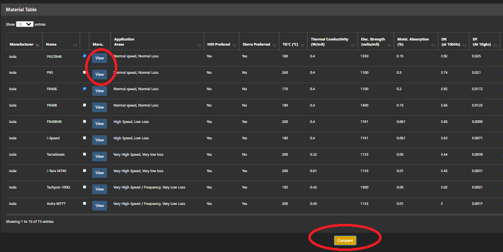
By clicking the “View” button, you can view the properties of that particular material. To compare the properties, select two different materials by clicking the checkbox and hitting the Compare button. A new window pops up comparing the properties of the chosen materials.
Halogen-free
Select the option Yes to list out halogen-free materials. If the option All is selected, the tool considers all the available materials present. This filter only applies to rigid materials.
Very high thermal conductivity
Thermal conductivity is the ability of a material to transfer heat by conduction. It is usually represented by the symbol K, and its units are W/mK (watts per meter per degree Kelvin)
Select the Very High Thermal Conductivity option if you require thermal conductivity greater than 1W/mK.
The key material properties that are used as a criterion for selection/filtering are categorized in the following table:
| Electrical properties | Thermal properties | Chemical properties | Mechanical properties |
| Dielectric constant (Dk) | Glass transition temperature (Tg) | Moisture absorption (%) | Tensile modulus (Mpsi) |
| Dissipation factor (Df)/ Loss tangent (Tanδ) | Decomposition temperature (Td) | CAF resistance | Tensile strength (Kpsi) |
| CTI class/Voltage | Thermal conductivity (K) | Flexural strength (Kpsi) | |
| Dielectric electrical strength (V/Mil) | Coefficient of thermal expansion (CTE) | ||
| Max signal frequency content (GHz) | |||
| Highest data transfer rate (Gbps) | |||
| Fastest signal rise/fall time (ns) |
Electrical properties
In this section, fill in the fields to narrow down the required material.
Speed/loss
Based on the operating frequency (speed) and associated loss, PCB materials are categorized as:
- Normal speed/normal loss
- Medium speed/medium loss
- High speed/low loss
- Very high speed/very low loss
Depending on your application, you can choose one of these 4 categories. Select option “All” to view all the materials available, irrespective of these categories.
The dissipation factor (Df) is the most important in determining the extent of signal loss in a PCB material; a higher value of Df leads to a higher loss. Furthermore, the signal loss also increases with the frequency or speed of operation. Therefore, for controlling the loss at high frequencies or high speeds, choose a PCB material with a low Df value. Thus, the range of Df values is the criteria for the above speed/loss categorization.
The dielectric constant (Dk) of a PCB material changes with frequency. Large variations of Dk with frequency cause larger signal distortion/rise time degradation, which becomes less acceptable for high-frequency or high-speed signals. Therefore, as the signal frequency or speed increases, it is desirable to have less variation in Dk with frequency. The need for less variation of Dk with frequency for low-loss PCB materials has been recognized and implemented by all board material manufacturers.
If you would like to learn more about losses in PCB transmission lines, see losses in PCB transmission lines.
Max signal frequency content (GHz), or fastest signal rise/fall time (ns), or highest data transfer rate (Gbps)
You can also choose the materials based on maximum signal frequency content (GHz)/fastest signal rise or fall time (ns)/highest data transfer rate (Gbps).
These 3 parameters are related to each other; if any one of the aforementioned values is specified, the material selection tool automatically calculates the remaining two values. For example, if you input the maximum signal frequency content, it automatically displays the corresponding values of the fastest signal rise/fall time (ns) and the highest data transfer rate (Gbps).
Dielectric constant (Dk)
The Dk of most PCB materials ranges from 2 to 10. To choose the appropriate range out of this, a slider button has been provided in the Material Selector.
The Dk of a PCB material largely determines the trace width of controlled impedance transmission lines on the circuit board; the greater the Dk value, the lesser the trace width will be for the same target controlled impedance value. A higher Dk value also leads to higher dielectric loss. In general, high-speed/low-loss materials have lower Dk values. Thus, Dk becomes an important electrical performance criterion for material selection. For normal speed/normal loss materials, the Dk varies considerably with frequency; for very high speed/very low loss materials, the Dk remains effectively constant with frequency. The Dk of the most commonly used board material- FR4- for example FR370HR- is 3.92 @ 10Ghz.
The values of Dk specified in our Material Selector are with a material’s resin content at 50% (as per IPC guidelines for the listing of properties in the material’s datasheet). Since Dk varies with frequency as well, we have used the values at 10 GHz in this tool.
The range of the above-mentioned properties can be set using the respective sliding button.
Dissipation factor (Df)
A material’s dissipation factor is the most important factor in determining the signal attenuation or signal loss, as signals travel along a PCB conductor or trace. The lower a material’s dissipation factor is, the lesser will be the signal loss. Thus, Df is the most important selection criterion from the signal loss perspective. The Df of FR4 material FR370HR is 0.025 @ 10Ghz.
The values of Df specified in our Material Selector are with a material’s resin content at 50% (as per IPC guidelines for the listing of properties in the material’s datasheet). Since Df varies with frequency as well, we have used the values at 10 GHz in this tool.
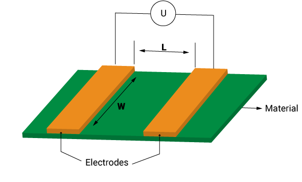
CTI class/voltage (comparative tracking index)
It is a measure of the voltage threshold above which electric breakdown can occur between 2 electrical conductors on the surface of a material. The smaller the CTI class value, the higher the threshold voltage. The CTI of the most commonly used PCB material- FR4- for example FR370HR- is CTI Class 3 with the electric breakdown voltage range being 175V-249V.
Dielectric electrical strength
Electrical strength, given in volts per unit thickness, measures the maximum electrical field a board material can withstand in the Z direction before its electrical breakdown. In this tool, the unit used is volts/mil. The dielectric electrical strength of the most commonly used PCB material- FR4- for example, FR370HR- is 1350 V/mil. Most of the IPC-certified materials have a dielectric electrical strength >= 750 V/mil.
Volume resistivity
It is the electrical resistance of any material of unit length and unit cross-sectional area (A) when measured across the length (l). Volume resistivity is expressed in units of Ω-cm (ohm-cm). For a dielectric material, since resistivity is very high, it is usually expressed in units of MΩ-cm. The volume resistivity of FR4 material, for example, FR370HR, is 3.0 x 10⁸ MΩ-cm.
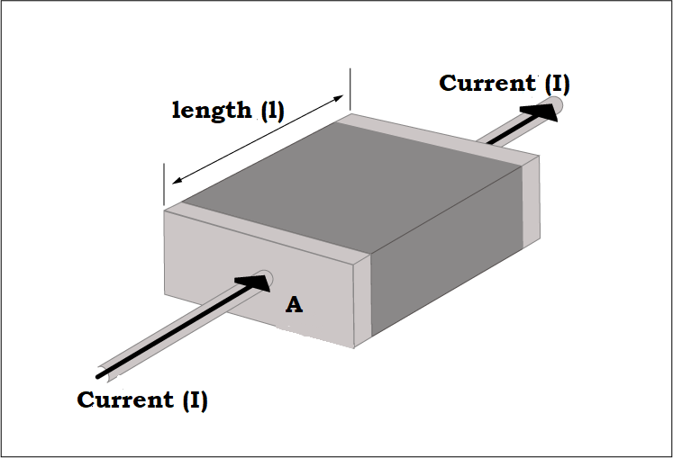
Resistance R = ρ⋅ (L/A); where ρ is the resistivity
The inverse of volume resistivity is called electrical conductivity (σ), which is expressed in Mhos/cm or Siemens/cm.
Surface resistivity
It is the electrical resistance of any material surface of a square shape of any dimension when measured across one of the dimensions. Surface resistivity is expressed in units of ohms or ohms per square. For a dielectric material, since resistivity is very high, it is usually expressed in units of Mohms or Mohms per square. The surface resistivity of the most commonly used PCB material FR4- for example, FR370HR- is 3.0 x 10⁶ MΩ-cm.
Resistance R = ρₛ(L/W); where ρ is the resistivity
Arc resistance
The ability of an insulating material (measured in terms of time) to withstand a high-voltage electric arc and resist the formation of a conducting path along its surface. The conducting path is due to the chemical and thermal decomposition of the material. For example, the arc resistance of FR4 material FR370HR is 115 seconds.
Dielectric breakdown
It is the voltage at which breakdown of a dielectric material occurs, usually expressed in kV. The dielectric breakdown voltage of FR4 – FR370HR is 50kV.
Thermal properties
In this section, you can set the range of various thermal properties like glass transition temperature (Tg), decomposition temperature (Td), coefficient of thermal expansion (CTE) along X, Y, and Z axes, and thermal conductivity (K).
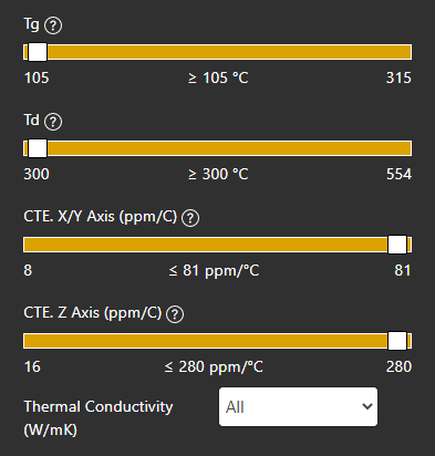
Glass transition temperature (Tg)
Tg is the temperature around which a circuit board substrate transitions from a glassy, rigid state to a softened, deformable state. Above Tg, the material has a substantially higher coefficient of thermal expansion than that below Tg. However, the deformation with temperature around Tg is completely elastic; when the temperature drops from a temperature higher than Tg to below Tg, the material returns to its original state. For all lead-free (ROHS compatible) materials, the Tg requirement is >= 170 °C. The Tg of FR4 material FR370HR is 180 °C.
Decomposition temperature (Td)
Td is the temperature at which a PCB material chemically decomposes, and the change is completely irreversible; once the material crosses Td, it cannot return to its original state after cooling down and therefore becomes totally non-functional. The Td of FR4 material FR370HR is 340 °C.
Coefficient of thermal expansion (CTE) X/Y and Z direction
It is the rate of expansion of a board material in the X, Y, and Z directions as the temperature increases. These values refer to the rate of expansion below Tg. The X, Y CTE of FR4 material FR370HR is (13,14) ppm/°C. The Z-axis CTE of FR370HR is 45 ppm/°C.
Thermal conductivity
The unit of thermal conductivity (K) is W/mK (Watt per meter per degree Kelvin). The K of most PCB materials is in the range of 0.2 to 0.5 W/m⋅K; for FR4 material FR370HR, it is 0.4 W/mK.
Based on the values of thermal conductivity, we have categorized them into 3 categories, as given in the drop-down list:
- Normal (≤ 0.5 W/mK)
- High (0.5 to 1 W/mK)
- Very high (> 1 W/mK)
Time to delamination- T260
The amount of time, in minutes, a dielectric material can withstand before failure or delamination at 260°C. The T260 time of FR4- for instance, FR370HR- is 60 minutes.
Time to delamination- T288
The amount of time, in minutes, a dielectric material can withstand before failure or delamination at 288°C. The T288 time of FR370HR is 30 minutes.
Chemical properties
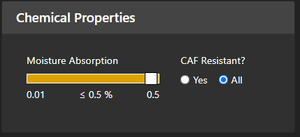
Here, you can set the range of tolerable moisture absorption of the required material. If a CAF-resistant material is required, you can select the option “Yes” else select the option “All”.
Moisture absorption
It is a measure of the ability of a board material to resist water absorption when immersed in water. It is given by the percentage increase in weight of a dielectric material due to water absorption under controlled conditions as specified in the IPC test method standard IPC-TM-650- 2.6.2.1A. The moisture absorption of FR4 material FR370HR is 0.15%.
CAF resistance
CAF (conductive anodic filament) is a metallic filament that is formed due to electrochemical migration. Formation of CAF might lead to electrical failure. This can be avoided by choosing CAF-resistant materials. Opt for CAF-resistant materials if your circuit board operates under a high-temperature and high-power environment.
Methylene chloride resistance
It is a measure of a material’s chemical resistance; specifically, the ability of a circuit board material to resist methylene chloride absorption.
Just like moisture absorption, it is expressed by a percentage increase in the weight of a PCB material due to exposure to or soaking in methylene chloride under controlled conditions. Most board materials have methylene chloride resistance values in the range of 0.01% to 0.20%.
Flammability
UL94, or the standard for the safety of flammability of plastic materials, is defined by Underwriter Laboratories. Most PCB materials adhere to UL94 V-0, whose main requirement is that the specimens may not burn with flaming combustion for more than 10 seconds after each application of the test flame.
Mechanical properties
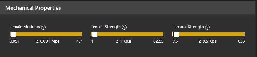
Mechanical properties (tensile modulus, tensile strength, and flexural strength) of the required material can be set in this section. The two common units of measurement listed for mechanical properties are Mpa (Megapascals) and Kpsi (Kilopounds per square inch). If the datasheet of a material only lists one unit, you can convert between the two using:
1 Mpa = 0.145 Kpsi
1 Kpsi = 6.895 Mpa = 0.703 kg/m²
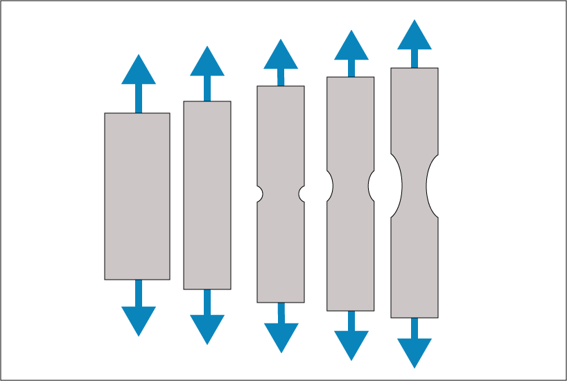
Often, there are 2 numbers given when reading the mechanical properties of a material. The mechanical properties exhibit slightly different values in 2 perpendicular directions, namely- MD (Machine Direction) and CD (Cross Direction). The MD is typically the direction that is fed lengthwise into a machine (X-axis), while the CD is perpendicular (Y-axis) to the MD. MD and CD apply to those PCB materials that have the glass-fiber cloth as a reinforcement in the resin system.
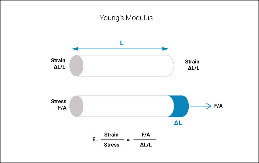
Tensile modulus (Young’s modulus)
It’s a measure of the mechanical strength (and possibly stiffness) of a PCB material. It measures the stress/strain ratio in the same direction that force (tensile or compressive) is applied. Young’s modulus is also correlated to the stiffness of a material.
The unit of stress is the same as that of pressure, i.e., force per unit area. Strain, being the ratio of two lengths, is dimensionless. Therefore, the unit of tensile modulus is the same as that of stress, i.e., force per unit area. The most commonly used units are Mpsi (Megapounds per square inch) in the Imperial System and Gpa (Gigapascals) in the Metric System. They are related as:
1 Mpsi=6.895 Gpa
The tensile modulus of FR4 material FR370HR is 3.744 Mpsi (MD) and 3.178 Mpsi (CD).
Tensile strength
The maximum tensile stress a material will withstand while being stretched or pulled before permanent, irreversible deformation in the form of necking takes place. The cross-section starts to significantly contract at the necking site. The tensile strength of the most commonly used PCB material- FR4- for example, FR370HR- is 55.9 Kpsi (MD) and 35.62 (CD).
Flexural strength
Flexural strength is a measure of a material’s tendency to bend under load. It is measured as the maximum load per unit area that a material will withstand without fracturing (permanent bending), when supported at the ends and loaded at the center, as shown in the diagram below.
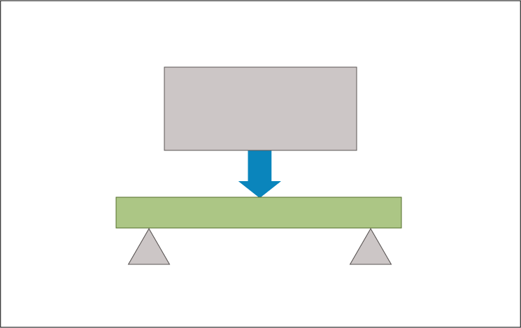
For homogenous materials, flexural strength is the same as tensile strength, and for composite materials (which most PCB materials are), flexural strength is usually higher than tensile strength. The flexural strength of PCB material FR4- FR370HR- is 90 Kpsi (MD) and 77 Kpsi (CD).
Poisson’s ratio
It is the ratio of the strain in the transverse direction to the strain in the direction in which the load is applied. The Poisson’s ratio of the most commonly used PCB material- FR4- for example FR370HR- is 0.177 (MD) and 0.171 (CD).
Dimensional stability
The amount of dimensional change a dielectric material can undergo when exposed to different degrees of temperature. The units are usually expressed in mm/m or mils/in. The dimensional stability of Rogers 4350 B, for example, is < 0.5 mm/m or mils/in.
Peel strength
It is the measure of the bond strength between the copper conductor and the dielectric material. It is expressed in pounds of force per linear inch (PLI, or average load per conductor width) required to separate bonded materials where the angle of separation is 180 degrees. The peel strength of FR370HR is 1.14 N/mm or 6.5 lb/in.
IPC and slash number
Using this option, the right IPC standard applicable to your circuit board can be selected.
The electrical performance of the signal traces is affected by the materials used in the circuit board. Sierra Circuits’ PCB Material Selector tool assists you in comparing and selecting the materials that best meet your design requirements.
How to select the best PCB material

Sierra Circuits has developed easy-to-use tools for PCB Designers and Electrical Engineers at every stage of circuit board development.


Fabrication, Procurement, & Assembly. PCBs fully assembled in as fast as 5 days.
- Bundled together in an entirely-online process
- Reviewed and tested by Engineers
- DFA & DFM Checks on every order
- Shipped from Silicon Valley in as fast as 5 days

Fabrication. Procurement & Assembly optional. Flexible and transparent for advanced creators.
- Rigid PCBs, built to IPC-6012 Class 2 Specs
- 2 mil (0.002″) trace / space
- DFM Checks on every order
- 24-hour turn-times available

Complex technology, with a dedicated CAM Engineer. Stack-up assistance included.
- Complex PCB requirements
- Mil-Spec & Class 3 with HDI Features
- Blind & Buried Vias
- Flex & Rigid-Flex boards