Speak to an Account Manager
![]() +1 (800) 763-7503
+1 (800) 763-7503

Get a quote for your rigid PCBs
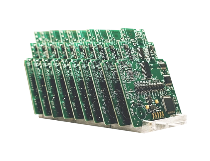
Transform your PCB manufacturing experience with Sierra Circuits, your trusted partner for top-notch rigid PCBs. Whether you require a straightforward single-layer circuit board with rapid delivery or a sophisticated 30-layer mil-spec PCB featuring exotic metals, we have you covered. Sierra Circuits is your go-to solution for an instant quote and swift manufacturing, with the capability to deliver your boards in as little as 48 hours.
- Manufactured in Silicon Valley
- On-site inventory of the finest materials
- Up to 30 layers
- 2-day turn-times available
- Component procurement
- PCB assembly
What sets Sierra Circuits apart is our commitment to excellence. All our PCBs are manufactured in Silicon Valley, ensuring proximity to cutting-edge technology and materials. Our on-site inventory boasts the finest materials, allowing us to meet your requirements for up to 30 layers of precision and complexity. Experience the advantage of a 1-day turn-time for your projects, providing unmatched speed without compromising quality.
A reliable partner for your manufacturing needs
With Sierra Circuits, you’re not just getting circuit boards; you’re gaining a reliable partner for your manufacturing needs. We prioritize customer satisfaction and aim to exceed expectations at every step. Our experienced team is ready to collaborate with you, ensuring that your rigid PCBs meet the highest standards of quality and reliability.
Whether you’re a seasoned professional or a newcomer to the world of PCBs, Sierra Circuits is here to simplify the manufacturing process. Our user-friendly quote system streamlines the initial steps, providing you with the information you need promptly. Trust Sierra Circuits for your rigid board needs and experience the convenience, speed, and precision that sets us apart in the industry.

Sierra Circuits supports IPC-2581.
IPC-2581 stands as a cornerstone standard in the manufacturing of your rigid PCBs, transforming the dynamics of design data exchange. Its open, vendor-neutral format enhances communication efficiency, providing a comprehensive platform for sharing crucial details like layer stack-up and drill specifications. Embracing IPC-2581 not only fosters superior collaboration but also minimizes errors during data transfer, ultimately elevating the precision and reliability of the entire fabrication process.
Product Promise
Sierra Circuits manufactures and assembles your rigid PCBs with full intellectual property protection.
PCB highlights:
- Up to 30 layers
- Board thickness: .005″ – .300″
- Max panel size: 21″ x 30″
- Min trace and space: .002″
- Solder mask feature tolerance: .001″
- Blind and buried vias
Fabrication highlights:
- Routed arrays
- Edge plating
- Bevels
- Heat sinks
PCB classifications:
- IPC 6012, class 1, 2 and 3
- MIL-PRF-55110
- MIL-PRF-31032/1
- MIL-PRF-31032/2
Quality management systems:
- AS9100D
- ISO 9001:2015
- ISO 13485:2016
Board parameters for rigid PCBs |
|||||||||||||||||||||||||||||||||||||||||||||||||||||||||||||||||||||||||||||||||||||||||||||||||||
| STANDARD | ADVANCED | MICRO | |||||||||||||||||||||||||||||||||||||||||||||||||||||||||||||||||||||||||||||||||||||||||||||||||
| Min Layer Count | 1 | 1 | 1 | ||||||||||||||||||||||||||||||||||||||||||||||||||||||||||||||||||||||||||||||||||||||||||||||||
| Max Layer Count | 30 | 30 | 30 | ||||||||||||||||||||||||||||||||||||||||||||||||||||||||||||||||||||||||||||||||||||||||||||||||
| Min Board Thickness | .010” (.254 mm) | .005” (.127 mm) | .005” (.127 mm) | ||||||||||||||||||||||||||||||||||||||||||||||||||||||||||||||||||||||||||||||||||||||||||||||||
| Max Board Thickness | .300” (7.62 mm) | .300” (7.62 mm) | .300” (7.62 mm) | ||||||||||||||||||||||||||||||||||||||||||||||||||||||||||||||||||||||||||||||||||||||||||||||||
| Min Core Thickness | .004” (.102 mm) | .002” (.051 mm) | .002” (.051 mm) | ||||||||||||||||||||||||||||||||||||||||||||||||||||||||||||||||||||||||||||||||||||||||||||||||
| Min Dielectric | .004” (.102 mm) | .003” (.076 mm) | .002″ (.051 mm) | ||||||||||||||||||||||||||||||||||||||||||||||||||||||||||||||||||||||||||||||||||||||||||||||||
| Min Starting Copper Foil Weight | 3 microns | 3 microns | 3 microns | ||||||||||||||||||||||||||||||||||||||||||||||||||||||||||||||||||||||||||||||||||||||||||||||||
| Max Finished Copper Thickness (O/L) | 4 oz (118 ml) | 6 oz (177 ml) | 1 oz (30 ml) | ||||||||||||||||||||||||||||||||||||||||||||||||||||||||||||||||||||||||||||||||||||||||||||||||
| Max Finished Copper Thickness (I/L) | 4 oz (118 ml) | 4 oz (118 ml) | 0.5 oz (15 ml) | ||||||||||||||||||||||||||||||||||||||||||||||||||||||||||||||||||||||||||||||||||||||||||||||||
| Min Panel Size | 12” x 18” (30 x 46 cm) | 12” x 18” (30 x 46 cm) | 12″ x 18″ (30 x 46 cm) | ||||||||||||||||||||||||||||||||||||||||||||||||||||||||||||||||||||||||||||||||||||||||||||||||
| Max Panel Size | 12” x 18” (30 x 46 cm) | 21” x 29” (53 x 74 cm) | 18″ x 24″ (46 x 61 cm) | ||||||||||||||||||||||||||||||||||||||||||||||||||||||||||||||||||||||||||||||||||||||||||||||||
| Smallest Mechanical Drill Diameter | .0059” (.150 mm) | .0059” (.150 mm) | .0059″ (.150 mm) | ||||||||||||||||||||||||||||||||||||||||||||||||||||||||||||||||||||||||||||||||||||||||||||||||
| Smallest Laser Drill Diameter | .005″ (.127 mm) | .004″ (.102 mm) | .004″ (.102 mm) | ||||||||||||||||||||||||||||||||||||||||||||||||||||||||||||||||||||||||||||||||||||||||||||||||
| Min Finished Hole Size | .004” (.102 mm) | .002” (.051 mm) | .002″ (.051 mm) | ||||||||||||||||||||||||||||||||||||||||||||||||||||||||||||||||||||||||||||||||||||||||||||||||
| Max Through Hole Aspect Ratio (depending on board thickness and finish hole) | 10:1 | 10:1 | > 20:1 | ||||||||||||||||||||||||||||||||||||||||||||||||||||||||||||||||||||||||||||||||||||||||||||||||
| Max Laser Via Aspect Ratio | .75:1 | .75:1 | .9:1 | ||||||||||||||||||||||||||||||||||||||||||||||||||||||||||||||||||||||||||||||||||||||||||||||||
| Blind Via Finished Hole Size | .004” (.102 mm) | Plated Shut | Plated shut | ||||||||||||||||||||||||||||||||||||||||||||||||||||||||||||||||||||||||||||||||||||||||||||||||
| Buried Via Finished Hole Size | .004” (.102 mm) | .002” (.051 mm) | .002″ (.051 mm) | ||||||||||||||||||||||||||||||||||||||||||||||||||||||||||||||||||||||||||||||||||||||||||||||||
| Min Trace and Space | .004” (.102 mm) | .003” (.076 mm) | .002″ (.051 mm) | ||||||||||||||||||||||||||||||||||||||||||||||||||||||||||||||||||||||||||||||||||||||||||||||||
| Min Pad Size for Test | .005” (.127 mm) | .005” (.127 mm) | .005″ (.127 mm) | ||||||||||||||||||||||||||||||||||||||||||||||||||||||||||||||||||||||||||||||||||||||||||||||||
| Process Pad Diameter | D + .012” (.305 mm)
(1-mil (.025-mm) annular ring) |
D + .004” (.102 mm) (tangency) | D + .004” (.102 mm) (tangency) | ||||||||||||||||||||||||||||||||||||||||||||||||||||||||||||||||||||||||||||||||||||||||||||||||
| Stacked Vias | Yes | Yes | Yes | ||||||||||||||||||||||||||||||||||||||||||||||||||||||||||||||||||||||||||||||||||||||||||||||||
| Min Wire Bond Pad Size | > .006” (.152 mm) | .004” (.102 mm) | .004″ (.102 mm) | ||||||||||||||||||||||||||||||||||||||||||||||||||||||||||||||||||||||||||||||||||||||||||||||||
| Controlled Impedance Tolerance | 10% | 5% | 5% | ||||||||||||||||||||||||||||||||||||||||||||||||||||||||||||||||||||||||||||||||||||||||||||||||
| Solder Mask Registration | .002” (.051 mm) | .001” (.025 mm) | .001″ (.025 mm) | ||||||||||||||||||||||||||||||||||||||||||||||||||||||||||||||||||||||||||||||||||||||||||||||||
| Solder Mask Feature Tolerance | .0015” (.038 mm) | .001” (.025 mm) | .001” (.025 mm) | ||||||||||||||||||||||||||||||||||||||||||||||||||||||||||||||||||||||||||||||||||||||||||||||||
| Solder Mask Min Dam Size (based on green soldermask color) | .005” (.127 mm) | .004” (.102 mm) | .004″ (.102 mm) | ||||||||||||||||||||||||||||||||||||||||||||||||||||||||||||||||||||||||||||||||||||||||||||||||
| Min Diameter Route Cutter Available | .024” (.610 mm) | .021” (.533 mm) | .021″ (.533 mm) | ||||||||||||||||||||||||||||||||||||||||||||||||||||||||||||||||||||||||||||||||||||||||||||||||
| Routed Part Size Tolerance | .005” (.127 mm) | .003” (.076 mm) | .003″ (.076 mm) | ||||||||||||||||||||||||||||||||||||||||||||||||||||||||||||||||||||||||||||||||||||||||||||||||
| Laser Hole Location Tolerance | .0005” (.013 mm) | .0005” (.013 mm) | .0005″ (.013 mm) | ||||||||||||||||||||||||||||||||||||||||||||||||||||||||||||||||||||||||||||||||||||||||||||||||
| Laser Routed Part Size Tolerance ( can only be done with panels < .032” thick) | .001” (.025 mm) | .001” (.025 mm) | .001″ (.025 mm) | ||||||||||||||||||||||||||||||||||||||||||||||||||||||||||||||||||||||||||||||||||||||||||||||||
| Bow and Twist Tolerance | Per IPC spec | Per IPC spec | Per IPC spec | ||||||||||||||||||||||||||||||||||||||||||||||||||||||||||||||||||||||||||||||||||||||||||||||||
| Thickness Tolerance (based on board thickness) | 10% | 5% | 5% | ||||||||||||||||||||||||||||||||||||||||||||||||||||||||||||||||||||||||||||||||||||||||||||||||
| Sequential Laminations | 3 or less lamination cycles | 4 lamination cycles | 5 lamination cycles | ||||||||||||||||||||||||||||||||||||||||||||||||||||||||||||||||||||||||||||||||||||||||||||||||
| Buried Vias | Yes | Yes | Yes | ||||||||||||||||||||||||||||||||||||||||||||||||||||||||||||||||||||||||||||||||||||||||||||||||
| Blind Vias | Yes | Yes | Yes | ||||||||||||||||||||||||||||||||||||||||||||||||||||||||||||||||||||||||||||||||||||||||||||||||
| Conductive Filled Vias | Yes | Yes | Yes – Cu plate shut | ||||||||||||||||||||||||||||||||||||||||||||||||||||||||||||||||||||||||||||||||||||||||||||||||
| Non Conductive Filled Vias | Yes | Yes | Yes | ||||||||||||||||||||||||||||||||||||||||||||||||||||||||||||||||||||||||||||||||||||||||||||||||
Surface finish parameters for rigid PCBs |
|||||||||||||||||||||||||||||||||||||||||||||||||||||||||||||||||||||||||||||||||||||||||||||||||||
| STANDARD | ADVANCED | MICRO | |||||||||||||||||||||||||||||||||||||||||||||||||||||||||||||||||||||||||||||||||||||||||||||||||
| HASL (Vertical or Horizontal) | Yes | Yes | No | ||||||||||||||||||||||||||||||||||||||||||||||||||||||||||||||||||||||||||||||||||||||||||||||||
| Lead Free HASL | Yes | Yes | No | ||||||||||||||||||||||||||||||||||||||||||||||||||||||||||||||||||||||||||||||||||||||||||||||||
| OSP (Shikoku F2) | Yes | Yes | Yes | ||||||||||||||||||||||||||||||||||||||||||||||||||||||||||||||||||||||||||||||||||||||||||||||||
| OSP (Entek) | Yes | Yes | Yes | ||||||||||||||||||||||||||||||||||||||||||||||||||||||||||||||||||||||||||||||||||||||||||||||||
| ENIG (Electroless Nickel/Immersion Gold) | Yes | Yes | Yes | ||||||||||||||||||||||||||||||||||||||||||||||||||||||||||||||||||||||||||||||||||||||||||||||||
| Immersion Silver | Yes | Yes | No | ||||||||||||||||||||||||||||||||||||||||||||||||||||||||||||||||||||||||||||||||||||||||||||||||
| Electrolytic Soft Gold | Yes | Yes | Yes | ||||||||||||||||||||||||||||||||||||||||||||||||||||||||||||||||||||||||||||||||||||||||||||||||
| Electrolytic Hard Gold | Yes | Yes | Yes | ||||||||||||||||||||||||||||||||||||||||||||||||||||||||||||||||||||||||||||||||||||||||||||||||
| Selective Gold | Yes | Yes | Yes | ||||||||||||||||||||||||||||||||||||||||||||||||||||||||||||||||||||||||||||||||||||||||||||||||
Solder mask finish parameters for rigid PCBs |
|||||||||||||||||||||||||||||||||||||||||||||||||||||||||||||||||||||||||||||||||||||||||||||||||||
| STANDARD | ADVANCED | MICRO | |||||||||||||||||||||||||||||||||||||||||||||||||||||||||||||||||||||||||||||||||||||||||||||||||
| Semi – Glossy | Yes | Yes | Yes | ||||||||||||||||||||||||||||||||||||||||||||||||||||||||||||||||||||||||||||||||||||||||||||||||
| Glossy | Yes | Yes | Yes | ||||||||||||||||||||||||||||||||||||||||||||||||||||||||||||||||||||||||||||||||||||||||||||||||
| Matte | Yes | Yes | Yes | ||||||||||||||||||||||||||||||||||||||||||||||||||||||||||||||||||||||||||||||||||||||||||||||||
Solder mask color parameters for rigid PCBs |
|||||||||||||||||||||||||||||||||||||||||||||||||||||||||||||||||||||||||||||||||||||||||||||||||||
| STANDARD | ADVANCED | MICRO | |||||||||||||||||||||||||||||||||||||||||||||||||||||||||||||||||||||||||||||||||||||||||||||||||
| Green | Yes | Yes | Yes | ||||||||||||||||||||||||||||||||||||||||||||||||||||||||||||||||||||||||||||||||||||||||||||||||
| Black | Yes | Yes | Yes | ||||||||||||||||||||||||||||||||||||||||||||||||||||||||||||||||||||||||||||||||||||||||||||||||
| Red | Yes | Yes | Yes | ||||||||||||||||||||||||||||||||||||||||||||||||||||||||||||||||||||||||||||||||||||||||||||||||
| Blue | Yes | Yes | Yes | ||||||||||||||||||||||||||||||||||||||||||||||||||||||||||||||||||||||||||||||||||||||||||||||||
| Yellow | Yes | No | No | ||||||||||||||||||||||||||||||||||||||||||||||||||||||||||||||||||||||||||||||||||||||||||||||||
| White | Yes | No | No | ||||||||||||||||||||||||||||||||||||||||||||||||||||||||||||||||||||||||||||||||||||||||||||||||
| Clear | Yes | Yes | Yes | ||||||||||||||||||||||||||||||||||||||||||||||||||||||||||||||||||||||||||||||||||||||||||||||||
| Bright White | Yes | No | No | ||||||||||||||||||||||||||||||||||||||||||||||||||||||||||||||||||||||||||||||||||||||||||||||||
| Purple | Yes | No | No | ||||||||||||||||||||||||||||||||||||||||||||||||||||||||||||||||||||||||||||||||||||||||||||||||
Legend mask parameters for rigid PCBs |
|||||||||||||||||||||||||||||||||||||||||||||||||||||||||||||||||||||||||||||||||||||||||||||||||||
| STANDARD | ADVANCED | MICRO | |||||||||||||||||||||||||||||||||||||||||||||||||||||||||||||||||||||||||||||||||||||||||||||||||
| All Colors | Yes | Yes | Yes | ||||||||||||||||||||||||||||||||||||||||||||||||||||||||||||||||||||||||||||||||||||||||||||||||
Mechanical parameters for rigid PCBs |
|||||||||||||||||||||||||||||||||||||||||||||||||||||||||||||||||||||||||||||||||||||||||||||||||||
| STANDARD | ADVANCED | MICRO | |||||||||||||||||||||||||||||||||||||||||||||||||||||||||||||||||||||||||||||||||||||||||||||||||
| Routed Array | Yes | Yes | Yes | ||||||||||||||||||||||||||||||||||||||||||||||||||||||||||||||||||||||||||||||||||||||||||||||||
| V Score, Edge to Copper | .01” | .007” (.178 mm) | .007″ (.178 mm) | ||||||||||||||||||||||||||||||||||||||||||||||||||||||||||||||||||||||||||||||||||||||||||||||||
| V Score Angles | 35°, 45°, 60° | 35°, 45°, 60° | 35°, 45°, 60° | ||||||||||||||||||||||||||||||||||||||||||||||||||||||||||||||||||||||||||||||||||||||||||||||||
| Countersink | Yes | Yes | Yes | ||||||||||||||||||||||||||||||||||||||||||||||||||||||||||||||||||||||||||||||||||||||||||||||||
| Counterbore | Yes | Yes | Yes | ||||||||||||||||||||||||||||||||||||||||||||||||||||||||||||||||||||||||||||||||||||||||||||||||
| Bevel | Yes | Yes | Yes | ||||||||||||||||||||||||||||||||||||||||||||||||||||||||||||||||||||||||||||||||||||||||||||||||
| Milling | +/- .003” (.076 mm) | +/- .002” (.051 mm) | +/- .001” (.025 mm) | ||||||||||||||||||||||||||||||||||||||||||||||||||||||||||||||||||||||||||||||||||||||||||||||||
| Edge Castellation | Yes | Yes | Yes | ||||||||||||||||||||||||||||||||||||||||||||||||||||||||||||||||||||||||||||||||||||||||||||||||
| Edge Plating | Yes | Yes | Yes | ||||||||||||||||||||||||||||||||||||||||||||||||||||||||||||||||||||||||||||||||||||||||||||||||
| Heatsinks | No | Yes | No | ||||||||||||||||||||||||||||||||||||||||||||||||||||||||||||||||||||||||||||||||||||||||||||||||
Electrical testing for rigid PCBs |
|||||||||||||||||||||||||||||||||||||||||||||||||||||||||||||||||||||||||||||||||||||||||||||||||||
| STANDARD | ADVANCED | MICRO | |||||||||||||||||||||||||||||||||||||||||||||||||||||||||||||||||||||||||||||||||||||||||||||||||
| 10 Volt | Yes | Yes | Yes | ||||||||||||||||||||||||||||||||||||||||||||||||||||||||||||||||||||||||||||||||||||||||||||||||
| 40 Volt (Burn-In Boards) | Yes | Yes | Yes | ||||||||||||||||||||||||||||||||||||||||||||||||||||||||||||||||||||||||||||||||||||||||||||||||
| 250 Volt | No | Yes | Yes | ||||||||||||||||||||||||||||||||||||||||||||||||||||||||||||||||||||||||||||||||||||||||||||||||
| 500 Volt | No | Yes | Yes | ||||||||||||||||||||||||||||||||||||||||||||||||||||||||||||||||||||||||||||||||||||||||||||||||
| Hi Pot | No | Yes | Yes | ||||||||||||||||||||||||||||||||||||||||||||||||||||||||||||||||||||||||||||||||||||||||||||||||
Laminate material parameters for rigid PCBs |
|||||||||||||||||||||||||||||||||||||||||||||||||||||||||||||||||||||||||||||||||||||||||||||||||||
| STANDARD | ADVANCED | MICRO | |||||||||||||||||||||||||||||||||||||||||||||||||||||||||||||||||||||||||||||||||||||||||||||||||
| Arlon 85NT | No | Yes | No | ||||||||||||||||||||||||||||||||||||||||||||||||||||||||||||||||||||||||||||||||||||||||||||||||
| Bergquist | No | Yes | No | ||||||||||||||||||||||||||||||||||||||||||||||||||||||||||||||||||||||||||||||||||||||||||||||||
| Flexible Polyimide | No | Yes | Yes | ||||||||||||||||||||||||||||||||||||||||||||||||||||||||||||||||||||||||||||||||||||||||||||||||
| Hybrid Constructions | Yes | Yes | Yes | ||||||||||||||||||||||||||||||||||||||||||||||||||||||||||||||||||||||||||||||||||||||||||||||||
| Isola 370HR | Yes | Yes | Yes | ||||||||||||||||||||||||||||||||||||||||||||||||||||||||||||||||||||||||||||||||||||||||||||||||
| Isola FR406 | Yes | Yes | Yes | ||||||||||||||||||||||||||||||||||||||||||||||||||||||||||||||||||||||||||||||||||||||||||||||||
| Isola FR408 HR | Yes | Yes | Yes | ||||||||||||||||||||||||||||||||||||||||||||||||||||||||||||||||||||||||||||||||||||||||||||||||
| Isola P95 | Yes | Yes | Yes | ||||||||||||||||||||||||||||||||||||||||||||||||||||||||||||||||||||||||||||||||||||||||||||||||
| Isola P96 | Yes | Yes | Yes | ||||||||||||||||||||||||||||||||||||||||||||||||||||||||||||||||||||||||||||||||||||||||||||||||
| Iteq IT180 | Yes | Yes | Yes | ||||||||||||||||||||||||||||||||||||||||||||||||||||||||||||||||||||||||||||||||||||||||||||||||
| Nelco BT N5000 | Yes | Yes | Yes | ||||||||||||||||||||||||||||||||||||||||||||||||||||||||||||||||||||||||||||||||||||||||||||||||
| Nelco N4000-13 | Yes | Yes | Yes | ||||||||||||||||||||||||||||||||||||||||||||||||||||||||||||||||||||||||||||||||||||||||||||||||
| Nelco N4000-29 | Yes | Yes | No | ||||||||||||||||||||||||||||||||||||||||||||||||||||||||||||||||||||||||||||||||||||||||||||||||
| Nelco N7000-2 | Yes | Yes | Yes | ||||||||||||||||||||||||||||||||||||||||||||||||||||||||||||||||||||||||||||||||||||||||||||||||
| No Flow Prepreg | Yes | Yes | Yes | ||||||||||||||||||||||||||||||||||||||||||||||||||||||||||||||||||||||||||||||||||||||||||||||||
| Panasonic Megtron | Yes | Yes | Yes | ||||||||||||||||||||||||||||||||||||||||||||||||||||||||||||||||||||||||||||||||||||||||||||||||
| Panasonic R1755 | Yes | Yes | No | ||||||||||||||||||||||||||||||||||||||||||||||||||||||||||||||||||||||||||||||||||||||||||||||||
| Panasonic R1766 | Yes | Yes | Yes | ||||||||||||||||||||||||||||||||||||||||||||||||||||||||||||||||||||||||||||||||||||||||||||||||
| Polyclad Getek | Yes | Yes | Yes | ||||||||||||||||||||||||||||||||||||||||||||||||||||||||||||||||||||||||||||||||||||||||||||||||
| PSA Bond Film | No | Yes | Yes | ||||||||||||||||||||||||||||||||||||||||||||||||||||||||||||||||||||||||||||||||||||||||||||||||
| Rogers 3000 Series | Yes | Yes | No | ||||||||||||||||||||||||||||||||||||||||||||||||||||||||||||||||||||||||||||||||||||||||||||||||
| Rogers R4000 Series | Yes | Yes | No | ||||||||||||||||||||||||||||||||||||||||||||||||||||||||||||||||||||||||||||||||||||||||||||||||
| Rogers 5000 Series | Yes | Yes | No | ||||||||||||||||||||||||||||||||||||||||||||||||||||||||||||||||||||||||||||||||||||||||||||||||
| Rogers 6000 Series | Yes | Yes | No | ||||||||||||||||||||||||||||||||||||||||||||||||||||||||||||||||||||||||||||||||||||||||||||||||
| Rogers TMM | Yes | Yes | No | ||||||||||||||||||||||||||||||||||||||||||||||||||||||||||||||||||||||||||||||||||||||||||||||||
| Ventec VT47 | Yes | No | No | ||||||||||||||||||||||||||||||||||||||||||||||||||||||||||||||||||||||||||||||||||||||||||||||||
Available reports for rigid PCBs |
|||||||||||||||||||||||||||||||||||||||||||||||||||||||||||||||||||||||||||||||||||||||||||||||||||
| STANDARD | ADVANCED | MICRO | |||||||||||||||||||||||||||||||||||||||||||||||||||||||||||||||||||||||||||||||||||||||||||||||||
| Microsection | Yes | Yes | Yes | ||||||||||||||||||||||||||||||||||||||||||||||||||||||||||||||||||||||||||||||||||||||||||||||||
| Solderability | Yes | Yes | Yes | ||||||||||||||||||||||||||||||||||||||||||||||||||||||||||||||||||||||||||||||||||||||||||||||||
| X-Ray Fluorescence | Yes | Yes | Yes | ||||||||||||||||||||||||||||||||||||||||||||||||||||||||||||||||||||||||||||||||||||||||||||||||
| Ionic Contamination | Yes | Yes | Yes | ||||||||||||||||||||||||||||||||||||||||||||||||||||||||||||||||||||||||||||||||||||||||||||||||
| Time Domain Reflectometry Test (TDR) | Yes | Yes | Yes | ||||||||||||||||||||||||||||||||||||||||||||||||||||||||||||||||||||||||||||||||||||||||||||||||
| FAI | Yes | Yes | Yes | ||||||||||||||||||||||||||||||||||||||||||||||||||||||||||||||||||||||||||||||||||||||||||||||||
| Certificate of Compliance | Yes | Yes | Yes | ||||||||||||||||||||||||||||||||||||||||||||||||||||||||||||||||||||||||||||||||||||||||||||||||
UL certifications for rigid PCBs |
|||||||||||||||||||||||||||||||||||||||||||||||||||||||||||||||||||||||||||||||||||||||||||||||||||
| STANDARD | ADVANCED | MICRO | |||||||||||||||||||||||||||||||||||||||||||||||||||||||||||||||||||||||||||||||||||||||||||||||||
| 94VO | Yes | Yes | No | ||||||||||||||||||||||||||||||||||||||||||||||||||||||||||||||||||||||||||||||||||||||||||||||||
PCB certifications for rigid PCBs |
|||||||||||||||||||||||||||||||||||||||||||||||||||||||||||||||||||||||||||||||||||||||||||||||||||
| STANDARD | ADVANCED | MICRO | |||||||||||||||||||||||||||||||||||||||||||||||||||||||||||||||||||||||||||||||||||||||||||||||||
| MIL-PRF-55110 | Yes | No | No | ||||||||||||||||||||||||||||||||||||||||||||||||||||||||||||||||||||||||||||||||||||||||||||||||
| MIL-PRF-31032/1 | Yes | No | No | ||||||||||||||||||||||||||||||||||||||||||||||||||||||||||||||||||||||||||||||||||||||||||||||||
| MIL-PRF-31032/2 | Yes | No | No | ||||||||||||||||||||||||||||||||||||||||||||||||||||||||||||||||||||||||||||||||||||||||||||||||
| IPC 6012, Class 1, 2 and 3 | Yes | Yes | Yes | ||||||||||||||||||||||||||||||||||||||||||||||||||||||||||||||||||||||||||||||||||||||||||||||||
| ISO 9001:2015 | Yes | Yes | Yes | ||||||||||||||||||||||||||||||||||||||||||||||||||||||||||||||||||||||||||||||||||||||||||||||||
| ISO 13485:2016 | Yes | Yes | Yes | ||||||||||||||||||||||||||||||||||||||||||||||||||||||||||||||||||||||||||||||||||||||||||||||||
Trusted by innovators
Engineers at the world’s most innovative companies choose Sierra Circuits for the highest quality rigid PCB manufacturing and assembly, right here in the USA.


Sierra Circuits engineers and technicians have the experience to bring your rigid PCBs to life.
Whether you need a high-volume advanced PCB run or a low-volume quick turn PCB run, there’s a reason Sierra Circuits leads the industry in quality and performance. Our engineers and technicians manufacture and assemble the most reliable PCBs, right here in the United States.
Ideal for:
- PCB designers and electrical engineers building prototypes or bringing products to market
- Contract manufacturers who need fast, predictable lead times
- Purchasing teams who require pricing and supply-chain transparency
- Tinkerers, hobbyists, and builders developing IoT home automation devices
Full turnkey boards available:
- PCB fabrication
- Component procurement
- In-house assembly


Manufacturing Equipment at Sierra Circuits
Our 70,000 sqft state-of-the-art campus in the heart of Silicon Valley contains the most advanced equipment required for the manufacture and assembly of your PCBs. Whether you’re looking for standard quick turn PCBs or boards with the tightest tolerances, made from exotic metals, there’s a reason Sierra Circuits leads the industry in quality and performance.

Get started with Rigid PCBs
We can turn your standard technology PCBs in as fast as in 24 hours.
Start a Custom Quote

Fabrication, Procurement, & Assembly. PCBs fully assembled in as fast as 5 days.
- Bundled together in an entirely-online process
- Reviewed and tested by Engineers
- DFA & DFM Checks on every order
- Shipped from Silicon Valley in as fast as 5 days

Fabrication. Procurement & Assembly optional. Flexible and transparent for advanced creators.
- Rigid PCBs, built to IPC-6012 Class 2 Specs
- 2 mil (0.002″) trace / space
- DFM Checks on every order
- 24-hour turn-times available

Complex technology, with a dedicated CAM Engineer. Stack-up assistance included.
- Complex PCB requirements
- Mil-Spec & Class 3 with HDI Features
- Blind & Buried Vias
- Flex & Rigid-Flex boards