Speak to an Account Manager
![]() +1 (800) 763-7503
+1 (800) 763-7503

Order full turnkey PCBs, entirely online. Manufactured in the USA, fully assembled, and shipped in 5 days.
Our online platform provides real-time stock visibility with integrated suppliers for transparent pricing. Get an online quote for truly American made PCB fabrication, components, and assembly in less than 2 minutes.
- PCB fabrication
Your standard technology PCBs are fabricated to the highest quality, right in Silicon Valley - Component procurement
Turnkey PRO provides fast and efficient pricing with no hidden costs! - Assembly
We create an unbroken thread from design to delivery.
Sierra Circuits engineers and turnkey PCB build teams are always accessible and responsive from quote through production and shipping.
Sierra Circuits supports IPC-2581.
Product Promise
Rapid PCB prototyping service: PCBs manufactured and assembled as quickly as you need them. Sierra Circuits can provide full turnkey boards in as fast as 5 days!
Create your boards entirely online
- PCB fabrication
- Component procurement
- In-house assembly
Assembly Specs:
- Dedicated CAM engineer
- BOM check
- DFA check
- DFM check
- 100% net-list testing
Prototype More Effectively
- 1 – 100 fully assembled boards
- Built to IPC-6012 class 2 specs
- UL approved
- Standard FR-4 material with ENIG or HASL finish
Turnkey Pro Fabrication & Assembly Capabilities |
|||||||||||||||||||||||||||||||||||||||||||||||||||||||||||||||||||||||||||||||||||||||||||||||||||
| Board Type | Only rigid boards. Turnkey Pro service provides both fabrication and full assembly of your boards (including component procurement). | ||||||||||||||||||||||||||||||||||||||||||||||||||||||||||||||||||||||||||||||||||||||||||||||||||
|---|---|---|---|---|---|---|---|---|---|---|---|---|---|---|---|---|---|---|---|---|---|---|---|---|---|---|---|---|---|---|---|---|---|---|---|---|---|---|---|---|---|---|---|---|---|---|---|---|---|---|---|---|---|---|---|---|---|---|---|---|---|---|---|---|---|---|---|---|---|---|---|---|---|---|---|---|---|---|---|---|---|---|---|---|---|---|---|---|---|---|---|---|---|---|---|---|---|---|---|
| Board Shape | We expect boards to be generally rectangular in shape. Notches, cutouts and slots are allowed (some restrictions shown below). | ||||||||||||||||||||||||||||||||||||||||||||||||||||||||||||||||||||||||||||||||||||||||||||||||||
| Board Spec | Boards will be built to IPC-6012 class 2 spec. However, in this online offer, we do not provide any microsection certificates or IPC coupons to customers. | ||||||||||||||||||||||||||||||||||||||||||||||||||||||||||||||||||||||||||||||||||||||||||||||||||
| Fabrication of ITAR or Export Controlled jobs? | No, we do not process any ITAR or Export controlled orders in this service. Only send us files that are not ITAR controlled or have no export control restrictions. | ||||||||||||||||||||||||||||||||||||||||||||||||||||||||||||||||||||||||||||||||||||||||||||||||||
| RoHS Available? | Yes, your board can be RoHS if you choose RoHS-compliant surface finish (ENIG). You have an option to not have any RoHS markings on your board if you so choose. | ||||||||||||||||||||||||||||||||||||||||||||||||||||||||||||||||||||||||||||||||||||||||||||||||||
| Layers Allowed | 2 layers, 4 layers, 6 layers, 8 layers. | ||||||||||||||||||||||||||||||||||||||||||||||||||||||||||||||||||||||||||||||||||||||||||||||||||
| Laminations | Single lamination double-sided or multi-layer boards only. In this online offer, we do not provide boards that need multiple laminations or have HDI features. | ||||||||||||||||||||||||||||||||||||||||||||||||||||||||||||||||||||||||||||||||||||||||||||||||||
| Blind Vias | No. | ||||||||||||||||||||||||||||||||||||||||||||||||||||||||||||||||||||||||||||||||||||||||||||||||||
| Buried Vias | No. | ||||||||||||||||||||||||||||||||||||||||||||||||||||||||||||||||||||||||||||||||||||||||||||||||||
| Tented Vias | No | ||||||||||||||||||||||||||||||||||||||||||||||||||||||||||||||||||||||||||||||||||||||||||||||||||
| High-Density Interconnect (HDI) | No. In this online offer we only provide single lamination PCBs with through-hole vias. | ||||||||||||||||||||||||||||||||||||||||||||||||||||||||||||||||||||||||||||||||||||||||||||||||||
| Non-plated Holes | Yes. | ||||||||||||||||||||||||||||||||||||||||||||||||||||||||||||||||||||||||||||||||||||||||||||||||||
| Via-in-Pads | We can manufacture your PCBs that have via-in-pad features. An extra process of non-conductive filling will be done on all vias, to ensure good soldering at assembly. Such vias must be 6 mils or more in size. In Turnkey Pro service, we only offer 7 days, 10 days and 15 days turnkey when your board has via-in-pad features. | ||||||||||||||||||||||||||||||||||||||||||||||||||||||||||||||||||||||||||||||||||||||||||||||||||
| Data for PCBs | For PCBs: We prefer RS-274X extended Gerber format. If your file is not in RS-274X, send an aperture file. Please, see FAQs below for what files to include. | ||||||||||||||||||||||||||||||||||||||||||||||||||||||||||||||||||||||||||||||||||||||||||||||||||
| Data for Assembly | For assembly: You will need to upload your BOM (excel format) online for quoting. In the final package, we will need the assembly drawing and XY data also. See sample BOM format. | ||||||||||||||||||||||||||||||||||||||||||||||||||||||||||||||||||||||||||||||||||||||||||||||||||
| Turnkey Turntimes | 5 days, 7 days, 10 days and 15 days. | ||||||||||||||||||||||||||||||||||||||||||||||||||||||||||||||||||||||||||||||||||||||||||||||||||
| Cut-off Time | 5:00 PM. Day 0 begins when validation is done or the final consigned components are received, whichever is later. | ||||||||||||||||||||||||||||||||||||||||||||||||||||||||||||||||||||||||||||||||||||||||||||||||||
| Order Quantities | For most designs, any quantity from 2 through 100 assembled PCBs available. Some limitations apply based on the number of panels to be produced and the turntime expected. To enable this service for larger quantities, please contact WendyG@protoexpress.com. | ||||||||||||||||||||||||||||||||||||||||||||||||||||||||||||||||||||||||||||||||||||||||||||||||||
| Maximum Board Size | Must fit a 10″ x 16″ box. The area must be less than 150 square inches. | ||||||||||||||||||||||||||||||||||||||||||||||||||||||||||||||||||||||||||||||||||||||||||||||||||
| Minimum PCB Dimensions | .5″ | ||||||||||||||||||||||||||||||||||||||||||||||||||||||||||||||||||||||||||||||||||||||||||||||||||
| Maximum PCB Dimensions | 15.9″ | ||||||||||||||||||||||||||||||||||||||||||||||||||||||||||||||||||||||||||||||||||||||||||||||||||
| Material | FR4, FR4-lead free. Standard materials are instantly quoted online. Exotic materials may be quoted by a specialist offline. Please note that this service is for rigid PCBs only. For flex or rigid-flex PCBs, please get a custom quote directly through a Sierra sales person. | ||||||||||||||||||||||||||||||||||||||||||||||||||||||||||||||||||||||||||||||||||||||||||||||||||
| Thickness & Thickness Tolerance | 0.062″, 0.031″ or 0.093″ with thickness tolerance of +/- 10%. | ||||||||||||||||||||||||||||||||||||||||||||||||||||||||||||||||||||||||||||||||||||||||||||||||||
| Arrays | Arrayed designs are not allowed. Your PCB design must have just a single image of a single board. (Our engineers will array it as needed for Sierra assembly and finally ship you fully-assembled individual boards.) | ||||||||||||||||||||||||||||||||||||||||||||||||||||||||||||||||||||||||||||||||||||||||||||||||||
| Minimum Trace/Space | 4 mils | ||||||||||||||||||||||||||||||||||||||||||||||||||||||||||||||||||||||||||||||||||||||||||||||||||
| Standard Copper Overplate | Surface pattern: Nominal 1 oz/sq foot. (0.0013″ to 0.002″) (33 microns to 51 microns) | ||||||||||||||||||||||||||||||||||||||||||||||||||||||||||||||||||||||||||||||||||||||||||||||||||
| Outer Layers Copper (Finished) | 1 oz or 2 oz (number of ounces of copper per square foot on outer layers.) Specify this as “finished” copper weight. 1 oz. is the most commonly-used finished copper weight. We start with ½ oz foil and plate up to 1 oz. If you specify 2 oz. as your finished copper weight, the minimum trace /space on your board must be at least 6 mils. | ||||||||||||||||||||||||||||||||||||||||||||||||||||||||||||||||||||||||||||||||||||||||||||||||||
| Inner Layers Copper | 1 oz | ||||||||||||||||||||||||||||||||||||||||||||||||||||||||||||||||||||||||||||||||||||||||||||||||||
| Maximum Number of Holes Per Board | 80 holes/square inch | ||||||||||||||||||||||||||||||||||||||||||||||||||||||||||||||||||||||||||||||||||||||||||||||||||
| Minimum Annular Ring Width | 0.006″ | ||||||||||||||||||||||||||||||||||||||||||||||||||||||||||||||||||||||||||||||||||||||||||||||||||
| Minimum Air Gap | 0.004″ (space between any two copper features) | ||||||||||||||||||||||||||||||||||||||||||||||||||||||||||||||||||||||||||||||||||||||||||||||||||
| Controlled Dielectric | In this online service, you cannot specify controlled dielectric, but we offer +/-10% controlled impedance (see below). | ||||||||||||||||||||||||||||||||||||||||||||||||||||||||||||||||||||||||||||||||||||||||||||||||||
| Controlled Impedance | This means in your design, you are specifying the width of certain traces and spacing to achieve a specific resistance. In your impedance modeling, use the Dk for material 370HR. We expect that, in your fab drawing, you will have an impedance table that CLEARLY identifies the target impedance(s), the layer(s) on which they exist and the specific trace widths/spaces to be controlled. See a sample format for impedance table. Do note that in this online service, our controlled impedance offering has certain limitations: Only offered for boards up to 6 layers only available with +/- 10% tolerance. You can have controlled impedances on up to four different layers on your board. On any layer, you can have up to two different controlled impedances. Our engineers will meet your controlled impedance requirements using our own stack-up. (All we need is your controlled impedance info. We do not need and may not use any specific controlled dielectric information you provide.) If your controlled impedance requirements exceed this spec, please ask for a custom quote. | ||||||||||||||||||||||||||||||||||||||||||||||||||||||||||||||||||||||||||||||||||||||||||||||||||
| Multiple Parts in one design | To keep our online service low-priced and hassle-free, we keep it simple. We do not allow different PCB designs and multiple BOMs to be combined in one order. Our system can only accept design files for a single circuit board with a single BOM. We cannot merge BOMs, de-duplicate multiple BOMs, etc. | ||||||||||||||||||||||||||||||||||||||||||||||||||||||||||||||||||||||||||||||||||||||||||||||||||
| Solder mask | Solder masks are available in green, blue and black. They can be used on both sides. However, in this service, we only offer LPI solder masks. Note: Sierra only offer LPI solder mask in this service. If your design forces us to use laser direct imaging LPI (LDI-LPI) solder mask, we will contact you and get approval for a $500 extra charge on your order. | ||||||||||||||||||||||||||||||||||||||||||||||||||||||||||||||||||||||||||||||||||||||||||||||||||
| Legend / Silkscreen | White. | ||||||||||||||||||||||||||||||||||||||||||||||||||||||||||||||||||||||||||||||||||||||||||||||||||
| Notches, Cutouts and Slots | Up to 10 plated slots allowed per board. Up to 10 non-plated slots allowed per board. Up to 10 cutouts allowed per board. Up to 10 notches allowed per board. (If any of the above allowances are exceeded in your design, we can still process it for a minimum $100 extra lot charge on your order. We will get your approval before doing so.) Minimum inside radius (for any notch, cutout or slot) = 20 mil (0.02″). Minimum width (of any notch, cutout or slot) = 40 mil (0.04″). | ||||||||||||||||||||||||||||||||||||||||||||||||||||||||||||||||||||||||||||||||||||||||||||||||||
| Logo | Vendor markings include company logo, UL marking, flammability, etc. Such vendor markings will be put in silkscreen. | ||||||||||||||||||||||||||||||||||||||||||||||||||||||||||||||||||||||||||||||||||||||||||||||||||
| IPC coupons & Microsection reports | Not provided in this online offering. Only available in custom ordered products. | ||||||||||||||||||||||||||||||||||||||||||||||||||||||||||||||||||||||||||||||||||||||||||||||||||
| Electrical Testing | 100% net-list testing on every board. | ||||||||||||||||||||||||||||||||||||||||||||||||||||||||||||||||||||||||||||||||||||||||||||||||||
| Shipping Options | FedEx/UPS, Will Call. You can use your own FedEx/UPS account number. International shipments allowed. All duties, customs and tariff charges are the customer's responsibility. | ||||||||||||||||||||||||||||||||||||||||||||||||||||||||||||||||||||||||||||||||||||||||||||||||||
| Payment Terms | Credit card (PO allowed for select customers who have set up credit terms). Payment link convenience: If your purchasing department typically puts in credit card number, you can still place an order and our system will email a payment link to that person. Order will start when payment information is received. | ||||||||||||||||||||||||||||||||||||||||||||||||||||||||||||||||||||||||||||||||||||||||||||||||||
| Restrictions | If your board has via-in-pad features, only 7 days, 10 days and 15 days turnkey quotes allowed (you cannot quote for 5 days turnkey). If you want faster turn times, you may use our custom quote service). | ||||||||||||||||||||||||||||||||||||||||||||||||||||||||||||||||||||||||||||||||||||||||||||||||||
| Assembly Class Specs | IPC-A-610 class2 | ||||||||||||||||||||||||||||||||||||||||||||||||||||||||||||||||||||||||||||||||||||||||||||||||||
| Assembly of ITAR designated jobs? | No. | ||||||||||||||||||||||||||||||||||||||||||||||||||||||||||||||||||||||||||||||||||||||||||||||||||
| Assembly on both sides | Yes. | ||||||||||||||||||||||||||||||||||||||||||||||||||||||||||||||||||||||||||||||||||||||||||||||||||
| Minimum Passive Component Size | 0201 inches | ||||||||||||||||||||||||||||||||||||||||||||||||||||||||||||||||||||||||||||||||||||||||||||||||||
| BGA Minimum Pitch | 0.5 mm. BGAs cannot have more than one ball size nor more than one pitch. | ||||||||||||||||||||||||||||||||||||||||||||||||||||||||||||||||||||||||||||||||||||||||||||||||||
| Minimum Pitch of Other Components | 0.4 mm | ||||||||||||||||||||||||||||||||||||||||||||||||||||||||||||||||||||||||||||||||||||||||||||||||||
| Maximum number of Through-hole Components | 20 per board | ||||||||||||||||||||||||||||||||||||||||||||||||||||||||||||||||||||||||||||||||||||||||||||||||||
| Minimum Component Pad Size | Minimum 8 mils x 8 mils or 8-mil diameter | ||||||||||||||||||||||||||||||||||||||||||||||||||||||||||||||||||||||||||||||||||||||||||||||||||
| Not allowed in Turnkey Pro Service | Our Turnkey Pro online service provides standard assembly, and has the following limitations: Wire-bonding, conformal coating, underfills, staking, POP assembly, wire assembly, or cable assembly are not allowed. Rework like cutting traces, soldering wire jumpers, and cables onto the boards are not allowed. Assembly of special items like PEM nuts, turrets terminals, rivets, and press-fit connectors are not allowed. (To get any of these extra assembly features, please ask for a custom quote.) | ||||||||||||||||||||||||||||||||||||||||||||||||||||||||||||||||||||||||||||||||||||||||||||||||||
Trusted by innovators
Engineers and PCB designers at the world's most innovative companies choose Sierra Circuits for top quality PCBs.


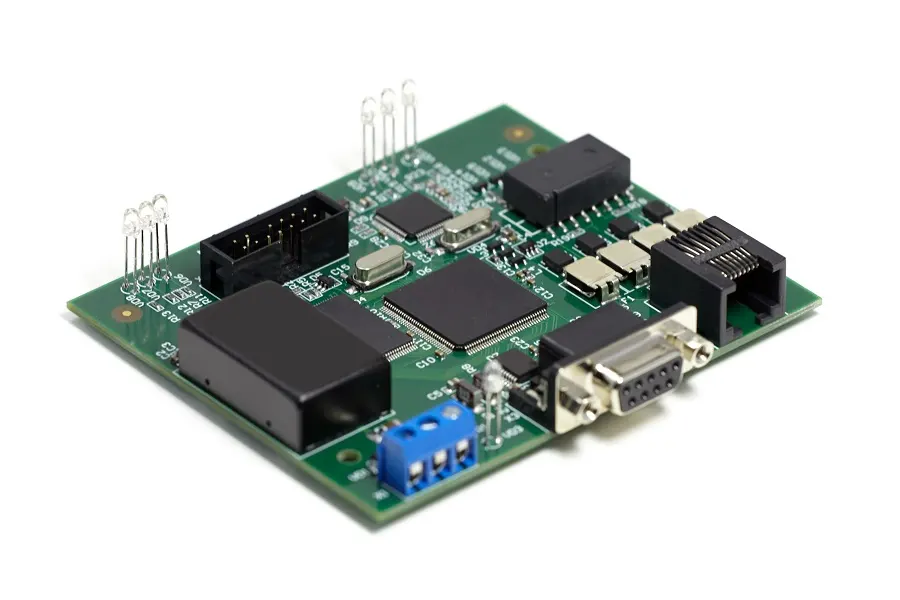
High-quality, high-performance PCBs. Fully assembled. Made to order. Ready to ship in as quick as 5 days.
Whether you’re an aerospace engineer on a tight deadline or a procurement officer looking to simplify your supply chain, Turnkey PRO is the most dependable full-service turnkey PCB solution.
Ideal for:
- PCB designers and electrical engineers building prototypes or bringing products to market.
- Contract manufacturers who need fast, predictable lead times.
- Purchasing teams who require pricing and supply-chain transparency.
- Tinkerers, hobbyists, and builders who would benefit from the expertise of our in-house CAM engineers.
Turnkey PRO also includes:
- PCB fabrication
- Component procurement
- In-house assembly


Manufacturing Equipment at Sierra Circuits
Our 70,000 sqft state-of-the-art campus in the heart of Silicon Valley contains the most advanced equipment required for the manufacture and assembly of your PCBs. Whether you’re looking for standard quick turn PCBs or boards with the tightest tolerances, made from exotic metals, there’s a reason Sierra Circuits leads the industry in quality and performance.

Get started with Turnkey PRO
Order our zero-defect rapid PCB prototyping service entirely online and get to market faster.
Start an Instant Online Quote

Fabrication, Procurement, & Assembly. PCBs fully assembled in as fast as 5 days.
- Bundled together in an entirely-online process
- Reviewed and tested by Engineers
- DFA & DFM Checks on every order
- Shipped from Silicon Valley in as fast as 5 days

Fabrication. Procurement & Assembly optional. Flexible and transparent for advanced creators.
- Rigid PCBs, built to IPC-6012 Class 2 Specs
- 2 mil (0.002″) trace / space
- DFM Checks on every order
- 24-hour turn-times available

Complex technology, with a dedicated CAM Engineer. Stack-up assistance included.
- Complex PCB requirements
- Mil-Spec & Class 3 with HDI Features
- Blind & Buried Vias
- Flex & Rigid-Flex boards