Via Design Techniques to Build Reliable PCBs

Amit Bahl
CRO
Sierra Circuits
Fill out the form:
Design techniques to build reliable PCB Vias
Designing reliable vias is crucial to building a successful PCB. It directly impacts the signal integrity of your circuit board. By optimizing these plated holes in your layout, you can ensure sufficient current-carrying capacity without overheating components or undesired voltage drops.
In this webinar, we will cover via design techniques.
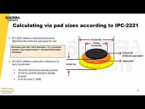
Precise calculation of via pad, hole, and annular ring dimensions is critical to eliminating the risk of annular ring breakout and drill wander. Always adhere to IPC-6012, IPC-2222, and IPC-2221 standards to make your vias manufacturable and durable. Maintain a balanced aspect ratio of 10:1 for through-holes and 0.75:1 for microvias to ensure uniform plating thickness and structural integrity.
When it comes to drilling, implement controlled depth for blind and buried vias to ensure the highest precision. Incorporate at least 10 mil of distance from the vias to the routed or scored edges to avoid board warping. The minimum drill-to-copper and pad-to-mask clearance should be 8 mil and 2.5 mil, respectively.
Via design without considering the required current rating might result in a high voltage drop in the traces. Our experts will demonstrate how Sierra Circuits’ Via Current Capacity and Temperature Rise Calculator can swiftly calculate the current rating based on the hole height and plating thickness.
You need to keep the via stub length as low as possible. Our designers will provide a live demo of an advanced design tool, the Maximum Via Stub Length Calculator, to determine the optimum stub length and its resonant frequency.
To avoid parasitic effects and signal reflections, the via impedance should match the trace impedance. Placing vias near heat-generating components and thermal pads can facilitate efficient heat transfer in your circuit.
Microsectional testing helps identify voids, cracks, delamination, and insufficient plating within the via structure. Whereas, interconnect stress testing (IST) can assess the vias’ ability to withstand mechanical stresses such as bending and vibration.
In this webinar, our design experts will demonstrate the techniques and best practices for designing efficient vias in PCBs.
What you’ll learn:
- Precision calculation of pad, hole, and annular ring sizes
- Via design techniques to ensure reliability
- Strategies to enhance the via current-carrying capacity
- Techniques to reduce unwanted stubs and impedance discontinuities
- Significance of thermal vias for effective heat transfer
- IST and microsectional test to check via reliability
- PCB design tool demos:
- Via Current Capacity and Temperature Rise Calculator
- Maximum Via Stub Length Calculator
This is a great opportunity to learn all about via design.
Presented by Amit Bahl
Amit has been in the PCB industry for 20+ years. He is the Chief Revenue Officer at Sierra Circuits. His passion is to empower tech companies to achieve their visions and change the world. Rockets going into space, self-driving cars taking up the streets, cancer-fighting medical devices, protecting the country, he’s ready to build any circuit board!
Watch the Trailer