Techniques for Building Reliable RF PCB Stack-Ups

Vandana CC
Engineering Project Coordinator
Sierra Circuits
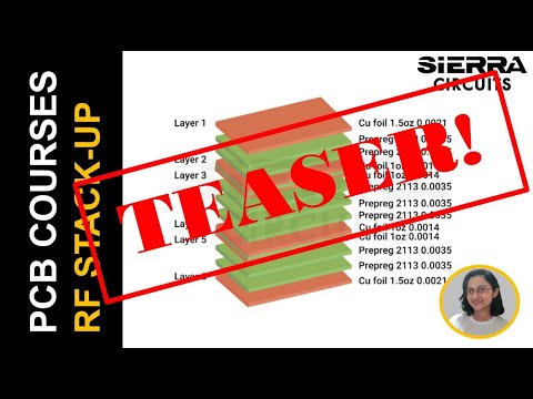
In high-frequency PCB designs, the stack-up is not just a structural element; it’s the foundation of your RF board’s performance. A poorly built-up stack-up might result in insertion loss, impedance discontinuities, skew, and electromagnetic interference. Whether you’re developing a basic prototype or an mmWave board, designing stack-ups with precision is critical to achieve signal fidelity.
In this webinar, you’ll learn practical techniques for designing RF PCB stack-ups that deliver consistent performance across various frequency ranges.
Practical strategies for designing high-performance radio-frequency stack-ups
Before choosing a stack-up, it’s essential to define your target operating frequency range, controlled impedance requirements, trace geometries, and grounding strategy.
Once the requirements are mapped out, the next step in designing RF PCB stack-ups is selecting the appropriate laminate. Choose materials with a stable and low dielectric constant (Dk) and a low dissipation factor (Df) to minimize insertion loss and phase distortion. Recommended RF materials include Rogers RO4350B (Dk=3.48, Df=0.0037 at 10 GHz), Isola Astra MT77 (Dk=3.0, Df=0.0017), or Panasonic Megtron 6 (Dk=3.35, Df=0.004 at 10 GHz).
After material selection, you should shift to the reference plane configuration. Ensure signal layers are tightly coupled to reference planes to minimize loop inductance and suppress common-mode radiation. To enhance shielding and field containment, add fencing or stitching vias. Ensure the via-to-via spacing doesn’t exceed λ/20, where λ is the operating wavelength.
An important consideration in designing radio-frequency stack-ups is selecting the appropriate transmission line structure. For many RF applications, grounded coplanar waveguides (GCPW) offer excellent field confinement and isolation. Microstrip and stripline configurations may also be suitable, depending on your stack-up and routing constraints.
To ensure your design is both functional and manufacturable, account for fabrication tolerances such as layer registration accuracy and dielectric thickness variations. Close collaboration with your manufacturer during the stack-up planning phase ensures material availability, impedance accuracy, and stack-up feasibility. As a best practice, document your stack-up in detail; include impedance targets, material specs, and layer assignments.
If you’re working on RF prototypes and want to ensure they’re ready for manufacturing, this webinar is for you.
In this session, we’ll guide you through real-world strategies for designing RF PCB stack-ups. Reserve your spot now and take the first step toward creating better RF boards.
What you’ll learn:
- Stack-up design can make or break your RF board
- How to select the best laminate for your prototypes
- How to arrange reference planes to prevent coupling
- RF stack-up configurations for transmission lines
- Tips to avoid board warping and mechanical stress
- Things you must include in your stack-up details
About Vandana CC
With a strong foundation in physics, Vandana CC brings a deep technical understanding to her work in PCB design and electronics manufacturing. She holds a Master’s in Physics and has experience teaching before transitioning into research at the Indian Institute of Science.
At Sierra Circuits, Vandana has played a key role in R&D projects, contributing to the development of engineering tools and calculators, technical content creation, and customer demos. Currently, she focuses on project coordination, ensuring seamless collaboration both within the team and with external partners. Her expertise bridges the gap between technical innovation and practical application, making her an integral part of Sierra Circuits’ engineering efforts.
Watch the Trailer