RF Design and Validation with VNA Demonstrations

Neil Jarvis
RF and Applications Engineer
Rohde & Schwarz

Amit Bahl
CRO
Sierra Circuits
When designing an RF PCB, selecting the right materials, optimizing stack-up, and maintaining signal integrity are essential. Even a minor oversight can lead to signal reflections, crosstalk, EMI, overheating, and system failure.
This webinar will guide you through the key aspects in RF PCB design and validation.
Critical considerations for radio-frequency board designs
Choosing the right laminate is crucial for ensuring the success of your RF boards. Select materials with a low dielectric constant (Dk < 4) and a low dissipation factor (Df < 0.005) to maintain signal quality and minimize losses. Due to their high-frequency operation, RF boards generate significant heat. For effective heat dissipation, use materials with high thermal conductivity (>0.5 W/mK).
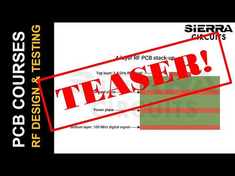
Stack-up is another critical aspect of RF board design and validation. Place signal layers adjacent to ground planes to minimize interference. To avoid board warpage and signal loss, always have a symmetrical build-up and incorporate RF traces and components on the outer layers.
To minimize signal reflection, design a continuous ground plane without any splits. Adjust the trace width, thickness, and clearance to achieve the desired characteristic impedance. Add stitching vias around the RF section to reduce parasitic inductance. The recommended spacing between these vias is λ/20, where λ is the operating wavelength.
To protect your board from external EM radiation, incorporate Faraday cages and ground pours around RF circuits. Ensure these ground pours do not create isolated ground islands; they can act as unintended antennas.
In addition to the above aspects, power supply noise is another important factor in RF PCB designs. To filter out high-frequency noise and provide a stable voltage supply, incorporate low ESR and ESL decoupling capacitors. Place these capacitors parallel to the signal path and as close as possible to the power supply pins of ICs.
In this webinar, our design experts will demonstrate the best RF PCB design and validation techniques to build a reliable circuit board.
Webinar agenda
5 key aspects of an RF design and validation:
- RF-compatible materials
○ Factors to consider
○ Guidelines for choosing an RF laminate
- Stack-up design
○ Best practices to build reliable RF layer stack
○ Hybrid stack-ups
- Ensuring signal integrity
○ RF transmission line and via design techniques to minimize crosstalk and EMI
○ Impedance matching to reduce reflections
○ Grounding and shielding strategies to mitigate EMI
- Power supply decoupling
○ Selection and placement of decoupling capacitors
- RF thermal management
○ Best practices and tips
Meet the speakers
Neil Jarvis
RF and Applications Engineer, Rohde & Schwarz
Neil Jarvis is known for his expertise in RF and microwave design, specializing in Vector Network Analysis and Spectrum Analysis. In his more than 22 years of experience in design engineering, test engineering and product development he’s held positions with National Semiconductor, Tagent Corporation, Northrop Grumman Corporation, and Agilent Technologies. In addition to his degrees in Math, EE, Technology Management and Systems Analysis, Neil holds multiple patents in RFID technology.
Amit Bahl
Chief Revenue Officer, Sierra Circuits
Amit Bahl, widely recognized as the PCB Guy, currently serves as the Chief Revenue Officer at Sierra Circuits. He earned his Bachelor of Science in Engineering from UCLA in 1997, launching his career in Silicon Valley’s tech industry. In 2009, he assumed the role of Director of Sales and Marketing at Sierra Circuits, with a dedicated focus on democratizing design for manufacturing best practices and guidelines for PCB designers and engineers.
Assuming the position of Chief Revenue Officer since 2022, Amit’s mission persists: to simplify the PCB design journey for all stakeholders. His unwavering dedication continues to drive Sierra Circuits as a trusted resource for the PCB design community.


