Resolving High-Speed PCB Design Challenges

Abhishek Chari
PCB Design Team Lead
Sierra Circuits
Designing a high-frequency circuit board is no joke; it requires precise technical knowledge and expertise in signal integrity, trace routing, and material selection.
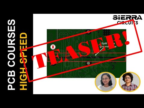
Sierra Circuits’ design team is capable of addressing high-speed PCB design challenges like achieving consistent line impedance, reducing signal reflections, and managing crosstalk between adjacent traces.
In this webinar, our PCB designers will demonstrate how we handle layout and design jobs for high-frequency circuits.
How Sierra Circuits’ PCB design team manages high-speed jobs
With years of experience in high-speed PCB design, our designers understand that the foundation lies in selecting the perfect materials for your prototypes. For instance, we know that substrates with a dielectric constant <4 and a dissipation factor <0.005 will help avoid insertion loss.
Being tied up with our in-house fabrication team, our design engineers understand the importance of matching the CTE values of the copper and laminate being considered in your prototype.
Not many know that by just doing this, you can eliminate the risk of board warping.
Having designed a plethora of high-speed boards, we understand how signal reflection, impedance discontinuities, and jitter can ruin your prototype’s functionality.
We thoroughly check for discontinuities and strategically route traces for optimum signal quality.
Generally, breaking out fine-pitch BGAs below 0.65 mm is considered quite challenging within tight space constraints. Our design experts gracefully handle these kinds of challenges by implementing breakout techniques like via-in-pad and microvia. We also balance complex escape routing with power integrity to meet electrical and fab requirements.
Sierra Circuits excels in designing high-speed interfaces like PCIe, DDR, and Ethernet. We incorporate fly-by topology for DDR3/4, tightly match PCIe differential pairs, and create Ethernet layouts with solid reference planes to avoid signal degradation.
In this webinar, our PCB design team will demonstrate two case studies on high-speed design. The first one covers via-in-pad routing and precise layer stack-up for an HDI board with 0.4 mm and 0.6 mm BGAs. The second case study highlights a complex high-frequency circuit with four DDR interfaces.
Overcoming high-speed PCB design challenges requires more than just theory; it demands hands-on expertise and the right partner. Sierra Circuits’ integrated design and fabrication workflow allows us to optimize every aspect of your board for reliability and manufacturability.
What you’ll learn:
- Sierra Circuits’ expertise in designing high-speed PCBs with live demos on:
o Choosing low-loss materials using the PCB Material Selector
o Handling high-frequency traces and reference planes
o Routing fine-pitch BGAs: strategies and clearances
o Designing with high-speed interfaces: PCIe, DDR, and Ethernet
- Case studies:
o HDI board with 0.4 and 0.6 mm pitch BGAs
o High-speed board with multiple DDRs
About Abhishek Chari
Abhishek Chari is the PCB Design Team Lead at Sierra Circuits. He began as an intern and quickly advanced to leading high-complexity PCB and embedded projects across commercial, medical, and defense sectors. His expertise spans 0.4mm pitch BGAs, high-voltage and high-current boards, custom stack-ups, and processor-based systems running Yocto Linux. Abhishek is known for tackling challenging designs under pressure and delivering robust hardware and embedded solutions.
Watch the Trailer