How to Protect Your RF Layouts from Noise and Signal Losses

Vandana CC
Engineering Project Coordinator
Sierra Circuits
Fill out the form:
If you want your RF layouts to perform reliably in the real world, you need to go beyond basic PCB design guidelines. You must analyze potential noise sources and make the right design decisions at the right time.
In this webinar, you will learn how to apply proven design techniques for protecting RF layouts from noise.
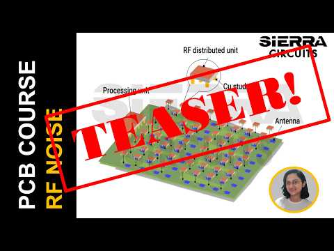
How to minimize noise in radio-frequency boards
To begin with, for a well-defined stack-up, you should always start by selecting appropriate dielectric materials. Consider using low-loss laminates such as Rogers or Megtron with a low dissipation factor (<0.005). You should also keep your RF signal layers adjacent to solid ground planes to avoid impedance discontinuities.
Do not overlook vias. Undesired stubs are a common source of signal degradation in RF designs. To counter these issues, you should use blind or buried vias whenever possible. If through-hole vias are unavoidable, keep stub lengths below 10 mil.
Grounding plays a critical role in protecting RF layouts from noise. A continuous, unbroken ground plane is essential. Avoid splits under RF traces, as even small gaps might cause impedance discontinuities.
You should appropriately terminate high-speed tracks to minimize signal reflections.
A series termination involves placing a resistor close to the driver. Whereas, in shunt termination, a resistor is connected in parallel with the receiver. The choice of termination depends on the application and the signal characteristics.
To validate your design, you can use time-domain reflectometry (TDR) and a vector network analyzer (VNA) to detect discontinuities in your transmission lines.
At the end of this session, you will be able to design RF boards that not only perform as expected but also consistently meet both electrical and manufacturing requirements.
Don’t miss out. Reserve your spot and elevate your RF layout design skill.
What you’ll learn:
- Designing reliable RF stack-ups for controlled impedance
- Crafting vias and minimizing via stubs
- Layout techniques to ensure uniform impedance across signal paths
- Component placement strategies for RF signal integrity
- Decoupling techniques to suppress power noise
- Managing return paths to reduce EMI
- Thermal considerations for maintaining RF performance stability
About Vandana CC
Engineering Project Coordinator at Sierra Circuits
With a strong foundation in physics, Vandana CC brings a deep technical understanding to her work in PCB design and electronics manufacturing. She holds a Master’s in Physics and has experience teaching before transitioning into research at the Indian Institute of Science.
At Sierra Circuits, Vandana has played a key role in R&D projects, contributing to the development of engineering tools and calculators, technical content creation, and customer demos. Currently, she focuses on project coordination, ensuring seamless collaboration both within the team and with external partners. Her expertise bridges the gap between technical innovation and practical application, making her an integral part of Sierra Circuits’ engineering efforts.
Watch the Trailer