How to Optimize Your Prototype for High-Volume PCB Manufacturing

Steve Bray
VP of Operations
Sierra Circuits

Orlen Bates
Sr. Field Application Engineer
EMA Design Automation
Fill out the form:
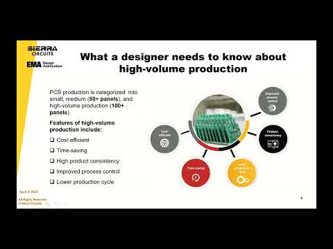
PCB production is categorized into small, medium (50+ panels), and high (100+ panels) volumes. The primary goal of high-volume production is to produce cost-effective and reliable boards with high yields. In bulk manufacturing, the risk of exceeding costs and lead time is high. To avoid this, efficient prototyping and testing are essential.
However, what worked in the prototype phase may not be applicable or economically feasible when moving into volume production. It is important to understand the different considerations for volume production to ensure successful manufacturing.
In this webinar, our PCB design and manufacturing experts will explain how to ease your transition from prototyping to high-volume production. This will help you eliminate the risk of board re-spins and reduce design expenditure.
What you will learn:
- How to achieve seamless transition from prototype to production
- Factors that affect cost and turnaround time
- PCB design considerations for a successful high-volume production
- Guidelines for choosing the right array and panel sizes.
- What designers often forget to convey to the fab house
- Tips on testing PCBs in large volumes
- How your vendor should be helping you to re-risk your supply chain for uninterrupted delivery
- How to leverage and use your CAD tools to design with high-volume in mind from the start
Presented by Steve Bray
Steve has been in the PCB and EMS industries for more than 20 years, holding executive positions in engineering, operations, quality, and supply chain. In the early part of his career, he worked in Europe and Asia, the latter in North America. Steve holds a Fellowship with the Institute of Circuit Technology, is a contributing member of the High Density Interconnect Group, and regularly consults with IPC subcommittee teams on emerging and diverging technologies.
And Orlen Bates
Orlen is a Sr. Field Application Engineer and has been in the field of PCB design since 1973 and has been with EMA since 2002. Orlen attended Vocational Tech School, earning a degree in Drafting & Design Technologies. With years of printed circuit (PCB), printed wire (PWB) design, DFM knowledge and high-volume manufacturing, Orlen is a highly skilled professional in the field of engineering physical design.
Watch the Trailer