How to Design High-Speed and High-Current PCB Traces

Amit Bahl
CRO
Sierra Circuits
Fill out the form:
Optimizing PCB trace design for high-speed and high-current applications
As technology advances, PCB designers and electrical engineers face new challenges in creating circuits with high frequencies and high current. This necessitates cutting-edge layout design techniques to prevent signal distortion and guarantee efficient power delivery without overheating.
In this webinar, you’ll learn the art of high-speed and high-current PCB trace design.
First, you must understand the distinct roles of signal, power, and ground traces. Signal lines should have uniform trace geometry and impedance for efficient data transmission. The power traces must handle high current without any voltage drop. Ground lines with a stable reference potential reduce noise in signal and power traces.
Stick to your contract manufacturer’s minimum/maximum line width capabilities to prevent open circuits and etching inconsistencies. Maintain 8 mil (minimum) drill-to-copper clearance to avoid short circuits.
To design high-speed PCB traces, calculate the critical length and 3 dB bandwidth. Computing the critical length allows you to identify trace sections where reflections and skew are most likely to occur. When a PCB trace has a sufficient 3 dB bandwidth, it allows all the harmonics and frequency components of the signal to propagate without distortion.
Our engineers will demonstrate how to calculate the critical length and 3 dB bandwidth for coated and uncoated microstrip configurations using the Bandwidth, Rise Time, and Critical Length Calculator.
Do not abruptly change the widths of the signal lines. Instead, gradually taper down traces with consistent spacing to achieve controlled impedance. Employ series and parallel termination resistors near the driver and receiver, respectively, to reduce signal reflections.
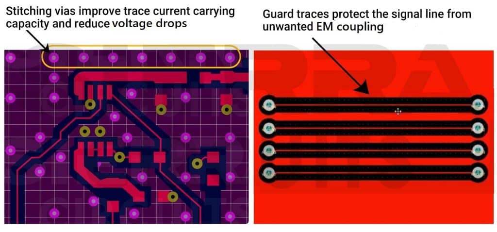
You can incorporate guard traces to protect the signal lines from unwanted EM coupling and suppress radiated EMI from the clock circuit. These traces are typically connected to the ground plane or dedicated reference voltage.
Implement ground stitching vias near the high-current traces to increase the current carrying capacity and reduce localized voltage drops.
When designing high-current boards operating above 10A, factors such as temperature rise over ambient, copper weight, trace current-carrying capacity, and resistance are paramount. The thicker the copper, the higher the ampacity. Use wider traces to handle high currents.
Our PCB design experts will provide a live demonstration of the Trace Width and Current Capacity Calculator. This tool instantly computes the ideal line width and temperature rise for a given current.
Thermal management is crucial in high-current PCB trace design. Copper pours around traces carrying high current can effectively dissipate the heat. Place thermal vias near the heat source to lower the thermal resistance and increase the heat dissipation rate.
Decoupling capacitors act as local reservoirs and prevent dips in the power supply voltage. The rule of thumb for decoupling capacitor placement is to position them as close as possible to the IC power and ground pins. Never route traces directly to the decoupling capacitors, as this results in additional trace length and circuit inductance.
In this webinar, you will learn various aspects of PCB trace design for demanding high-speed and high-current applications.
What you’ll learn:
- DFM guidelines for PCB trace design
- Designing signal lines for your current requirements
- Optimizing line characteristics for controlled impedance
- Techniques to achieve power integrity and signal integrity
- Sierra Circuits’ PCB design tool demos:
- Trace Width, Current Capacity, and Temperature Rise Calculator
- Bandwidth, Rise Time, and Critical Length Calculator
- High-speed and high-current trace design tips
- Advantages of multi-grid settings in your EDA tool
Meet the speaker
Amit Bahl, Chief Revenue Officer at Sierra Circuits
Amit Bahl, widely recognized as the PCB Guy, currently serves as the Chief Revenue Officer at Sierra Circuits. He earned his Bachelor of Science in Engineering from UCLA in 1997, launching his career in Silicon Valley’s tech industry. In 2009, he assumed the role of Director of Sales and Marketing at Sierra Circuits, with a dedicated focus on democratizing design for manufacturing best practices and guidelines for PCB designers and engineers.
Within a short span, Amit successfully propelled Sierra Circuits to become a leading educational platform for all aspects of PCBs. Under his leadership, Sierra expanded to offer blogs, design guides, webinars, calculators and design tools, and a vibrant forum, SierraConnect. Amit remains committed to ensuring the community has access to the essential resources, whether they are developing standard products or boards with specifications for medtech or military applications.
Assuming the position of Chief Revenue Officer since 2022, Amit’s mission persists: to simplify the PCB design journey for all stakeholders. His unwavering dedication continues to drive Sierra Circuits as a trusted resource for the PCB design community.
Watch the Trailer