High-Speed PCB Via Design and Manufacturing

Amit Bahl
CRO
Sierra Circuits

Ernie Frohring
Field Application Engineer
EMA Design Automation
Fill out the form:
Techniques to design high-speed PCB vias
It is undesirable to have vias for signals operating in the GHz range. If this is not possible, you need to optimize the number and position of vias in your board layout. The aim is to minimize impedance discontinuities and ensure a smooth signal transfer.
In this webinar, you’ll learn the following aspects of high-speed PCB via design.
When the via impedance doesn’t match the line impedance, it results in signal reflection and parasitic effects. To prevent this, you should position the ground vias near the signal vias to create an inductance loop for the return current. You can also implement coaxial via geometry to prevent impedance discontinuities.
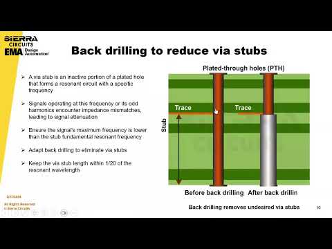
While placing vias on high-speed PCB traces, always keep the stub length as low as possible to manage signal attenuation. You need to ensure the signal’s maximum frequency is significantly lower than the stub fundamental resonant frequency. In addition to this, microvias offer more reliable signal transmission compared to through-hole vias.
In RF applications, via stitching ensures a continuous and low-impedance return path. Furthermore, to block EMI from reaching and coupling with the critical signals, employ via shielding to surround the sensitive signal traces with a barrier of ground vias or metal shielding.
To route DDRs in high-frequency circuits, a fly-by topology is ideal. It sequentially connects each memory module with the main controller, minimizing signal path length with fewer branches than T-topology.
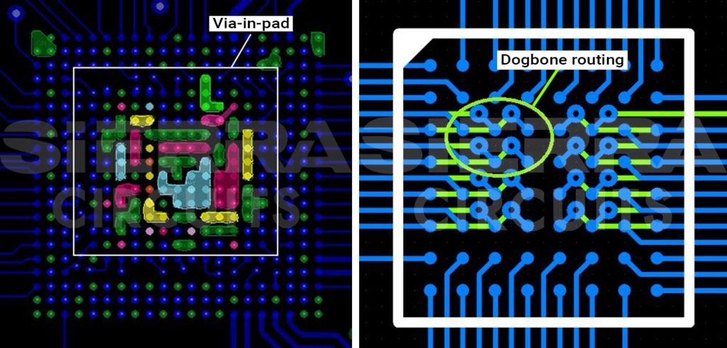
When breaking out 0.4 and 0.5 mm BGAs, incorporate via-in-pad. It involves placing multiple vias directly under the solder pad where the BGA ball is attached. Employ non-solder mask-defined pads if your design allows enough room between adjacent BGA pads.
To eliminate the risk of annular ring breakout and drill wander in high-speed PCB vias, precise annular ring calculation is crucial. Additionally, prefer staggered microvias over stacked if your board fabrication needs more than 3 lamination cycles. This will reduce the risks of barrel and corner cracking.
In this webinar, the EMA and Sierra experts will practically demonstrate the best practices for designing high-speed PCB vias.
Agenda:
1. Ways to reduce unwanted via stubs and impedance discontinuities
2. Via stitching and shielding
3. How to break out a BGA using via-in-pad and dogbone structures
4. DDR routing with fly-by and T-topology
5. Via filling and tenting
6. Price comparison: conductive and non-conductive via filling, standard via, back drilling
7. Sierra Circuits’ PCB design tools:
a. Via Impedance Calculator
b. Maximum Via Stub Length Calculator
And a demo by EMA of the effects of via stub length on signal integrity and attenuation.
Meet the speakers
Ernie Frohring
Field Application Engineer, EMA Design Automation
Ernie began his career in electronic design and instrumentation, specializing in emulators and logic analyzers. Since then, he has leveraged his knowledge of hardware instrumentation to become experienced in the software tools used for electronic design. He has worked with various PCB layout, schematic capture, analog simulation, and signal integrity analysis tools, and is especially interested in the integration of these tools into a design environment. He is currently specializing in RF and Digital simulation, doing presentations, and working one-on-one with customers using the EDA tools from Cadence and EMA Design Automation.
He graduated from Massachusetts Institute of Technology with a Bachelor’s and Masters degree in Electrical Engineering. His hobbies include chasing Total Solar Eclipses to interesting parts of the world.
Amit Bahl
Chief Revenue Officer, Sierra Circuits
Amit Bahl, widely recognized as the PCB Guy, currently serves as the Chief Revenue Officer at Sierra Circuits. He earned his Bachelor of Science in Engineering from UCLA in 1997, launching his career in Silicon Valley’s tech industry. In 2009, he assumed the role of Director of Sales and Marketing at Sierra Circuits, with a dedicated focus on democratizing design for manufacturing best practices and guidelines for PCB designers and engineers.
Within a short span, Amit successfully propelled Sierra Circuits to become a leading educational platform for all aspects of PCBs. Under his leadership, Sierra expanded to offer blogs, design guides, webinars, calculators and design tools, and a vibrant forum, SierraConnect. Amit remains committed to ensuring the community has access to the essential resources, whether they are developing standard products or boards with specifications for medtech or military applications.
Assuming the position of Chief Revenue Officer since 2022, Amit’s mission persists: to simplify the PCB design journey for all stakeholders. His unwavering dedication continues to drive Sierra Circuits as a trusted resource for the PCB design community.
Watch the Trailer