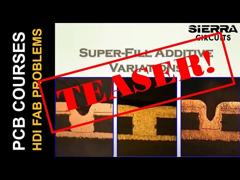
HDI Fabrication Problems, Quality Control and Reliability Issues

Happy Holden
50-year veteran of PCB technologies
Contributing Technical Editor of PCB007
The HDI fabrication problems you want to avoid
Early in our development of high-density interconnect technology, we encountered a lot of new HDI fabrication problems, as well as key design rules and useful stack-ups for designers and hardware engineers. You will get insights into how we solved these problems and lessons we learned for ‘Best Practices’. There are cautions that arise when fabricating an HDI-microvia board. This is one of three webinars that Sierra Circuits has selected from the myriad of HDI Workshops I have conducted over the years. It is intended to help companies successfully navigate the new and complex technology of high-density interconnects.
What you will learn:
HDI definitions, types and markets: Not all HDI products are the SAME!
History of HDI: It helps to understand why HDI was developed in 1982
HDI fabrication problems and issues: Some of the hurdles
- Via formation — mechanical and laser drilling quality- scoring quality in various materials
- Metallization — desmear, electroless copper, direct metalization and semi-additive processing
- Imaging and etching — achieving fine lines and spaces, controlled copper etch
- Electrodeposition — improved throwing power, enhancing through hole and microvia plating
- Reliability issues
- The use of coupons
How to develop a robust HDI process: Tools HP and others used for reliable HDI
HDI future: Ultra-HDI and next generation: Moving to Ultra-HDI and the new 3D HDI architecture
Additional references and reading: Free eBooks on HDI
Appendix of useful tools: Engineering Statistics Handbook
About Happy Holden
Happy Holden has spent over 50 years in printed circuit engineering, customer support and product development, with eight of those years in Taiwan, Hong Kong and China He was the CTO of the worlds largest PCB fabricator-Hon Hai Precision Industries-also known as FOXCONN. Prior, he was Senior PCB Technologist for Mentor Graphics’ System Design Division and Development Mgr. for Merix. Before retiring from Hewlett-Packard after 28 years, Holden was responsible for the creation and startup of the NanYa PCB facility in 1984, now the world’s largest organic FC IC substrate fabricator. Holden has a B.S. in chemical engineering from Oregon State University and an M.S. in EE/control theory.


