Design Considerations for an Error-Free PCB Stack-Up

Amit Bahl
CRO
Sierra Circuits
Fill out the form:
How to build an error-free PCB stack-up
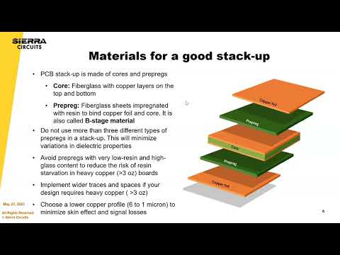
Designing an error-free PCB stack-up influences multiple factors such as signal integrity, controlled impedance, trace routing, and the board’s structural stability. A well-designed build-up optimizes the board’s electrical performance while minimizing cost and complexity. To realize this, you need to carefully estimate the number of signal, ground, and power layers and carefully arrange them. Dielectric material properties, type of construction (core/foil), and via placement are other important parameters to consider.
we’ll cover the following aspects to help you design an error-free PCB stack-up.
The type of technology (rigid, flex, HDI, or high-speed) also impacts the layer stack. For instance, HDI boards involve high-density routing with microvias in a compact space. Here, the vias influence the number of lamination cycles.
To maintain signal integrity, place solid ground planes right below the signal layers. This reduces crosstalk and EMI. For controlled impedance traces, the impedance should remain constant throughout the conductor to facilitate efficient transmission. To achieve this, you need to avoid placing vias on controlled impedance traces.
To lower the mechanical stress acting on the stack-up during the lamination process, you need to balance the copper weights in your build-up. If this is not done, it can lead to warpage or deformation.
Stack-up is a significant cost driver in your design. The higher the layers, the more expensive it is to manufacture. Adding 1 or 2 additional layers can increase the cost by 35% to 40%.
In this webinar on error-free PCB stack-up design, our experts will take you through the critical aspects of circuit board stack-up design that will help you build your prototype PCB.
What you’ll learn:
- Optimum layer estimation and arrangement
- HDI, flex, and high-speed stack-up considerations
- DFM guidelines for an efficient and error-free PCB stack-up
- Manufacturing tolerances
- How stack-up impacts signal integrity and controlled impedance
- Primary cost drivers of your build-up
- Fab notes: Stack-up details for your manufacturer
Presented by Amit Bahl
Amit has been in the PCB industry for 20+ years. He is the Chief Revenue Officer at Sierra Circuits. His passion is to empower tech companies to achieve their visions and change the world. Rockets going into space, self-driving cars taking up the streets, cancer-fighting medical devices, protecting the country, he’s ready to build any circuit board!
Watch the Trailer