Best PCB DFM Practices to Avoid Manufacturing Defects

Amit Bahl
CRO
Sierra Circuits

Patrick Davis
Product Management Director for Allegro
Cadence Design Systems

Vince Di Lello
Sr. Principal Product Engineer
Cadence Design Systems
Fill out the form:
PCB DFM practices for flawless fabrication
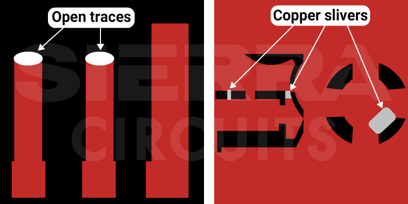
Following the PCB DFM practices optimizes the fabrication process as per your CM’s capabilities and reduces production costs. Design for manufacturing standards help identify potential manufacturing errors such as open traces, annular ring breakouts, copper slivers, and illegible silkscreen.
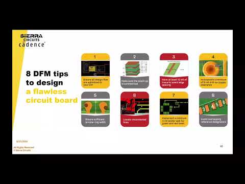
In this webinar, you will learn the following PCB design for manufacturing aspects:
First, you need to ensure all required fabrication data, such as Gerber, netlist, BOM, fab/assembly notes, and drill drawing, are submitted to your CM to avoid delay and iterative communication. Adopt the IPC-2581 format for design data exchange to facilitate smoother collaboration and faster turnaround time.
Choose materials that meet the design requirements, considering glass transition temperature (Tg), dissipation factor (Df), thermal conductivity (k), and mechanical strength. Ensure a symmetrical stack-up with 1 ground plane between 2 signal planes to prevent EMI.
Optimize the trace widths for high-current boards as per the copper weight and trace current-carrying capacity. Maintain at least 7 mil spacing between copper and board edges to avoid conductor corrosion.
Our experts will provide a live demonstration of Trace Width, Current Capacity and Temperature Rise Calculator. This tool will help you compute the ideal line width and temperature rise for a given current, instantly.
The standard aspect ratios for through holes and microvias are 10:1 and 0.75:1, respectively. When determining drill-to-copper clearance, consider the drilled hole edge. The recommended drill-to-copper to avert unintended connection is 8 mil.
To address breakout and tangency, provide 2 mil annular rings for laser drilled vias, 3 mil for mechanically drilled vias, and 5 mil for component holes.
Inappropriate clearance between the solder mask edge and surface features leads to solder bridges. Ensure the mask clearances are 2 mil larger than the copper pads, with a 1 mil annular ring. For green and red masks, have 4 mil of mask webs and 5 mil for other colors.
You need to position silkscreen texts beside the pad without overlapping. If not, it can hinder component identification. Implement silkscreen lines with a minimum width of 4 mil. Text height and length should be at least 25 mil to ensure legibility.
Sierra Circuits’ Better DFM tool will help you analyze the product design with optimum functionality. This tool ensures manufacturability and prevents re-spins by identifying design errors before production.
You will understand the practical DFM guidelines to streamline the PCB fabrication process in this webinar.
What you’ll learn:
● Common DFM errors
● PCB design for manufacturing guidelines for:
○ Manufacturing files
○ Circuit board stack-up
○ Trace width and spacing
○ Via and drilling
○ Solder mask and silkscreen
● Benefits of using IPC-2581
● Sierra Circuits advanced PCB design tools:
○ Trace Width, Current Capacity, and Temperature Rise Calculator
○ Better DFM
● Cadence True DFM demo
Level: Beginner
Meet the speakers
Amit Bahl, Chief Revenue Officer at Sierra Circuits
Amit Bahl, widely recognized as the PCB Guy, currently serves as the Chief Revenue Officer at Sierra Circuits. He earned his Bachelor of Science in Engineering from UCLA in 1997, launching his career in Silicon Valley’s tech industry. In 2009, he assumed the role of Director of Sales and Marketing at Sierra Circuits, with a dedicated focus on democratizing design for manufacturing best practices and guidelines for PCB designers and engineers.
Within a short span, Amit successfully propelled Sierra Circuits to become a leading educational platform for all aspects of PCBs. Under his leadership, Sierra expanded to offer blogs, design guides, webinars, calculators and design tools, and a vibrant forum, SierraConnect. Amit remains committed to ensuring the community has access to the essential resources, whether they are developing standard products or boards with specifications for medtech or military applications.
Assuming the position of Chief Revenue Officer since 2022, Amit’s mission persists: to simplify the PCB design journey for all stakeholders. His unwavering dedication continues to drive Sierra Circuits as a trusted resource for the PCB design community.
Patrick Davis, Product Management Director for Allegro at Cadence Design Systems
Patrick Davis is the Product Management Director for Allegro at Cadence Design Systems. He is an industry expert with over 25 years’ experience in the PCB design industry. Staring his career as a PCB designer and working his way up to Sr. Vice President of Design before pivoting to his new exciting role at Cadence Design Systems where he is helping define next generation of EDA tools for the engineering community.
Watch the Trailer