
Speak to an Account Manager
 +1 (800) 763-7503
RF / MW PCB Manufacturing and Assembly
Sierra Circuits specializes in the manufacturing and assembly of high-quality RF / MW PCBs.
We understand the material science behind the RF and microwave (10 MHz to 30 GHz) application requirements.
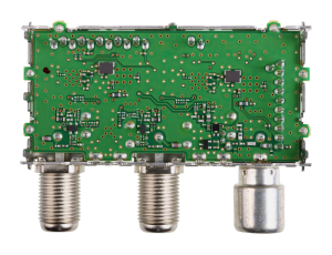
Why and Where Do You Need RF PCBs?
- Designed for high-frequency signal transmission with minimal loss and distortion.
- Offer superior impedance control and dielectric consistency for stable RF performance.
- Utilize specialized materials (PTFE, Rogers, or Taconic) to ensure low signal attenuation.
- Enable precise antenna integration for consistent radiation patterns and optimal signal strength.
Ideal for:
- Telecommunications – antennas, base stations, and 5G network modules.
- Aerospace and defense – radar, satellite communication, and navigation systems.
- Automotive – ADAS and vehicle radar sensors.
- IoT and wireless devices – RF modules, transceivers, and smart connectivity systems.
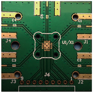
Why partner with Sierra Circuits for RF PCB manufacturing and assembly?
- Our fab engineers have extensive experience fabricating radio frequency circuit boards. We have perfected the process of supporting stack-ups, drilling, and etching.
- At Sierra Circuits, everything from material movement to feeding data to the machine is automated. The design rules are scripted into the system, making RF and microwave manufacturing more efficient with reduced human error.
- For precision, we utilize self-learning automated scaling software (XACT). This system analyzes material type, thickness, and copper weights on individual layers to provide a scaling prediction on material shrinkage. This data is used to improve the accuracy of the laser direct imaging and CO2 drilling system.
- We also have a mechanical vision drilling and routing machine that reduces errors by automatically realigning the board for multiple drill programs, which are often seen in via-in-pad and back drills.
- We have dedicated teams for DFM analysis, stack-up preparation, component sourcing, manufacturing, assembly, and testing. Once you place an order, these teams will collaborate seamlessly to deliver error-free prototypes.
| Stack-up | Stack-up | |||
|---|---|---|---|---|
| Minimum Layer Count | 2 |  | ||
| Maximum Layer Count | 30 | |||
| Minimum Board Thickness | 10 mil (0.010 in/0.254 mm) | |||
| Maximum Boards Thickness | 275 mil (0.275 in/6.985 mm) | |||
| Minimum Core Thickness | 3 mil (0.003 in/0.0762 mm) | |||
| Minimum Dielectric Thickness | 3 mil (0.003 in/0.0762 mm) | |||
| Thickness Tolerance (based on board thickness) | ±10% | |||
| Hybrid Constructions | PTFE and Non-PTFE based | |||
| Sequential Lamination | Up to 4 lamination cycles | |||
| Drill and Pad | Drill and Pad | |||
|---|---|---|---|---|
| Smallest Mechanical Drill Diameter | 5.9 mil (0.0059 in/0.150 mm) | 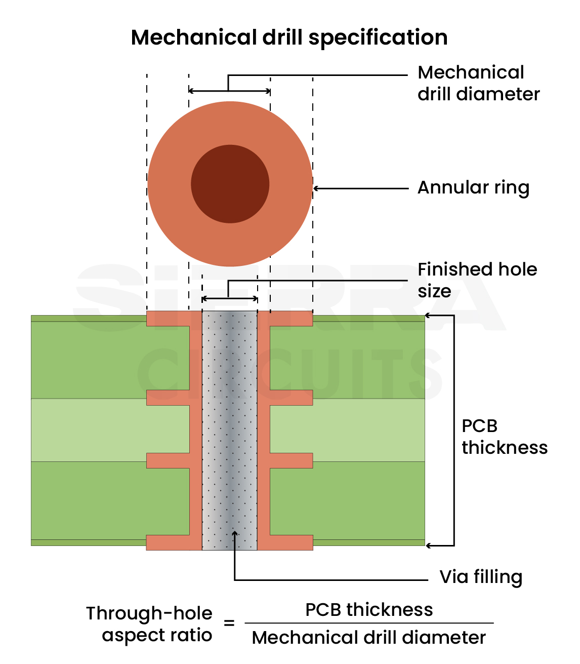  | ||
| Smallest Laser Drill Diameter | 4 mil (0.004 in/0.1016 mm) | |||
| Filled Vias (conductive and non Conductive) | Yes | |||
| Hole Treatment | Plasma and Sodium Etch | |||
| Blind Vias | Yes | |||
| Buried Vias | Yes | |||
| Stacked Vias | Yes | |||
| Maximum Through Hole Aspect Ratio (depends on the board thickness and finished hole size) | 10:1 | |||
| Maximum Laser Via Aspect Ratio | 0.75:1 | |||
| Minimum Pad Size for Test | 5 mil (0.005 in/0.127 mm) | |||
| Minimum Wire Bond Pad Size | >6 mil (0.006 in/0.1524 mm) | |||
| Backdrill to Copper Clearance | 10 mil (0.010 in/0.254 mm) | |||
| Backdrill to Backdrill Clearance | 6 mil (0.0060 in/0.152 mm) | |||
| Minimum Backdrill Oversize Diameter | 8 mil (0.0080 in/0.203 mm) to 10 mil (0.010 in/0.254 mm) | |||
| Minimum Controlled Depth Drilling | More than 1 mil (0.001 in/0.0254 mm) | |||
| Controlled Depth Drilling Tolerance | ±2 mil (0.002 in/0.0508 mm) | |||
| Trace and Spacing Clearances | Trace and Spacing Clearances | |||
|---|---|---|---|---|
| Minimum Trace Width | 3 mil (0.003 in/0.0762 mm) |  | ||
| Minimum Trace Space | 3 mil (0.003 in/0.0762 mm) | |||
| Controlled Impedance Tolerance | ±5% | |||
| Solder Mask and Surface Finish | Solder Mask and Surface Finish | |||
|---|---|---|---|---|
| Solder Mask Colors Available | Green, Red, and Blue |  | ||
| Solder Mask Registration | 2 mil (0.002 in/0.0508 mm) | |||
| Solder Mask Feature Tolerance | 1.5 mil (0.0015 in/0.0381 mm) | |||
| Solder Mask Minimum Dam Size |
| |||
| Solder Mask Finish | Semi–Glossy, Glossy, and Matte | |||
| Legend Colors Available | All Colors | |||
| Surface Finishes Available | ENIG, Immersion Tin, and ENEPIG | |||
| Selective and Full-Body Hard and Soft Gold Plating | Up to 120µ | |||
| Mechanical Parameters | Mechanical Parameters | |||
|---|---|---|---|---|
| Minimum Panel Size | 12”x18” |     | ||
| Maximum Panel Size | 12”x18” | |||
| Laser Routed Part Size Tolerance (Available for panels <0.032” thick) | 1 mil (0.001 in/0.0254 mm) | |||
| Minimum Diameter Route Cutter Available | 24 mil (0.024 in/0.6096 mm) | |||
| Routed Part Size Tolerance | 5 mil (0.005 in/0.127 mm) | |||
| Internal Cutouts, Slots | 5 mil (0.005 in/0.127 mm) | |||
| Routed Array | Yes | |||
| Countersink | Yes | |||
| Counterbore | Yes | |||
| Bevel | Yes | |||
| Milling | ±3 mil (0.003 in/0.0762 mm) | |||
| Edge Castellation | Yes | |||
| Gold Finger | Yes | |||
| Edge Plating | Yes | |||
| Heatsink | No | |||
| Recommended Laminate Materials | Recommended Laminate Materials | ||||
|---|---|---|---|---|---|
| RF Material | Material Type | Dk/Df Value (at 10 GHz) | |||
| RO4350 B | Ceramic-Filled PTFE | 3.48/0.0037 | |||
| RO4003 C | Ceramic-Filled PTFE | 3.38/0.0027 | |||
| RO3035 | Ceramic-Filled PTFE | 3.5/0.0015 | |||
| RO3003 | Ceramic-Filled PTFE | 3/0.001 | |||
| FR408HR | Multifunctional Epoxy | 3.65/0.0095 | |||
| I-Speed® | Multifunctional Epoxy | 3.63/0.0071 | |||
| I-Tera® MT40 (RF/MW) | Hydrocarbon-PPE | 3.45/0.0031 | |||
| Isola Astra MT77 | Hydrocarbon-PPE | 3/0.0017 | |||
| Tachyon-100G | Hydrocarbon-PPE | 3.02/0.0021 | |||
| Megtron6 R-5775 | Hydrocarbon-PPE | 3.35/0.004 | |||
| Component Assembly | Component Assembly | |||
|---|---|---|---|---|
| Component Compatibility | BGAs, QFNs, CSPs, 0201, 01005, 08004, POP, and press fit components |  | ||
| Fine-Pitch Assembly | Up to 13.8 mil (0.0138 in/0.35mm) | |||
| Solder Chemistry | Supports RoHS, Leaded, Indium, Clean, and No-clean Formulations | |||
| Paste-in-Hole | Compatible with through-hole solder paste applications | |||
| Cleaning Process | De-ionized water and chemical cleaning | |||
| Electrical Testing | 10 Volt and 40 Volt (burn-in boards) |  | ||
| Microsection | Yes | |||
| Solderability | Yes | |||
| X-Ray Fluorescence | Yes | |||
| Ionic Contamination | Yes | |||
| Time Domain Reflectometry Test (TDR) | Yes | |||
| First Article Inspection (FAI) | Yes | |||
| Certificate of Compliance | Yes | |||
PCB Testing and Reports
| PCB Certification | PCB Certification | |||
|---|---|---|---|---|
| MIL-PRF-55110 | Yes |  | ||
| MIL-PRF-31032/1 | Yes | |||
| MIL-PRF-31032/2 | Yes | |||
| IPC 6012, Class 1, 2 and 3 | Yes | |||
| ISO 13485:2016 | Yes | |||
| UL (94VO) | Yes | |||

RF PCB manufacturing and microwave prototyping challenges
Handling PTFE materials:
- Ceramic-filled PTFE materials are fragile and can easily break during the manufacturing process.
- Registration issues can also occur during lamination as they lack dimensional stability.
- Since PTFE laminates are soft, drill bits are likely to wander and break, so they need to be constantly replaced.
- Due to their non-stick properties, it is hard to plate copper or apply a solder mask.
- As PTFE materials are expensive, any manufacturing issues will significantly increase the lead time and cost.
Hence, it is crucial to partner with an RF PCB manufacturer who can address these challenges and fabricate your boards precisely.
Though working with non-PTFE materials is easier, handling high-frequency signals demands more design optimization. This requires your microwave PCB fabricator to stick to tighter tolerances.

RF material selection and stack-up preparation
At higher frequencies, the signal degrades due to insertion loss. This can occur due to conflicting dielectric properties, copper profile, and surface finish.
- Choose a low-tooth copper profile to avoid skin effects in your microwave and radio frequency circuits.
- Pick ENIG, immersion tin, or ENEPIG surface finish to prevent signal losses.
- Select a substrate with a low dielectric constant, low loss tangent, and stable electrical properties over a wide frequency range. Low Dk materials are usually PTFE-based, like Rogers RO4000 series or FR-4 with enhanced RF properties.
Before choosing the substrate, check its availability with your RF and microwave PCB manufacturer.
- A hybrid stack-up with mixed materials is also a viable option for RF/microwave designs. Here, go for low Dk laminates specifically for layers with critical traces and FR-4 for the rest. This provides better layer customization for signal integrity, thermal management, and signal isolation.
- Note that the chosen materials in hybrid stack-ups must have matching CTEs to avoid cracks during the lamination process.
At Sierra Circuits, we control curing parameters like temperature, pressure, and time to minimize inherent and residual stress, thus eliminating the risk of layer misalignment and delamination.

Optimizing your RF PCB and microwave circuit design
The key difference between RF and microwave PCBs is their operating frequencies. Radio frequencies range from 10 MHz to 1 GHz, while microwave frequencies are above 1 GHz.
At higher operating frequencies, circuit boards are prone to signal losses, EMI, crosstalk, ringing, and reflections.
Here are the top 6 microwave and RF circuit board design tips:
- Consider distributed and lumped elements when designing transmission lines in the RF frequency range. Generally, a 50Ω coplanar structure is used for minimum loss and maximum power transfer.
- Have a dedicated ground plane for each RF layer and implement ground stitching vias to distribute the ground connection.
- Apply DRC for stitching vias:
- Default via/pad clearance: 20 mil
- Minimum boundary clearance: 20 mil
- Incorporate decoupling capacitors and LC filters to suppress high-frequency noise.
- Choose materials with a dielectric constant of 3-3.5 and a loss tangent of 0.0022-0.0095 for minimal signal loss.
- Match the impedance of traces, components, and antennas to minimize signal reflections.
How to Place an Order for RF PCBs (with assembly)

Trusted by innovators
Engineers at the worlds most innovative companies choose Sierra Circuits for the highest quality RF/MW PCB manufacturing and assembly, right here in the USA.


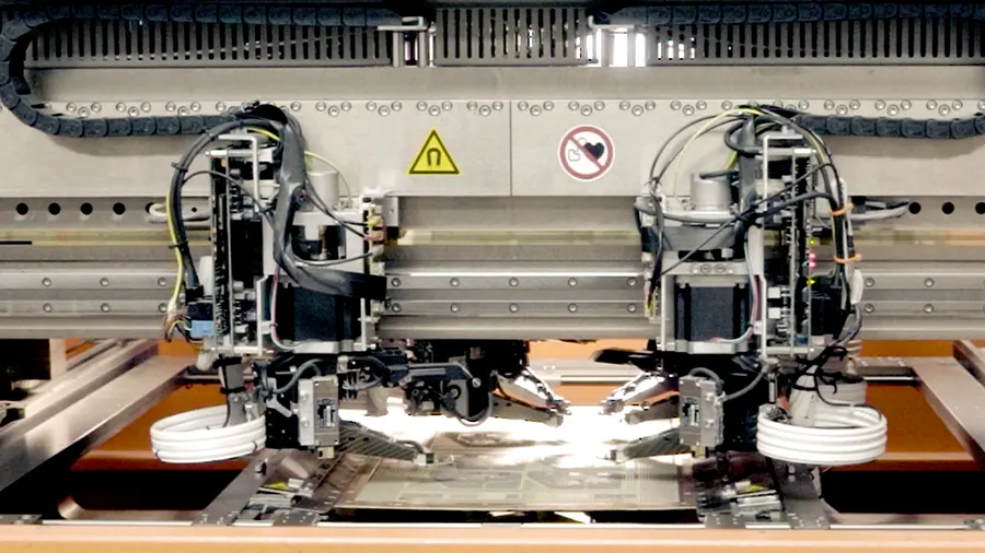
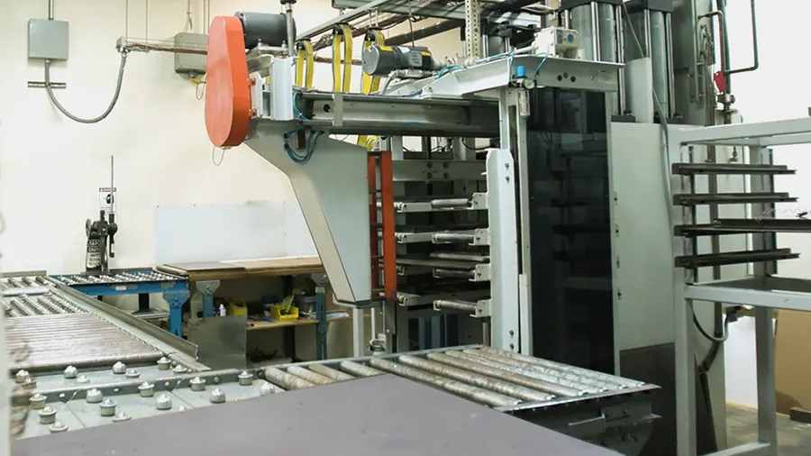
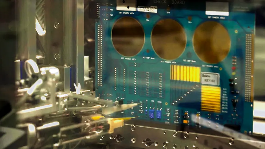
Manufacturing Equipment at Sierra Circuits
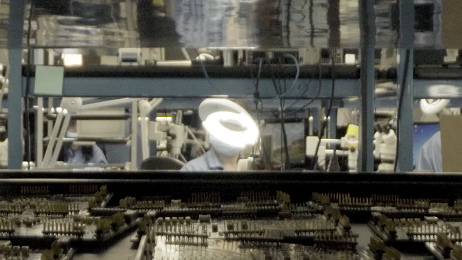
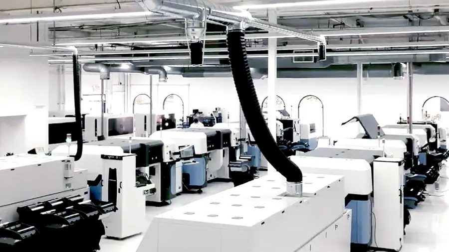
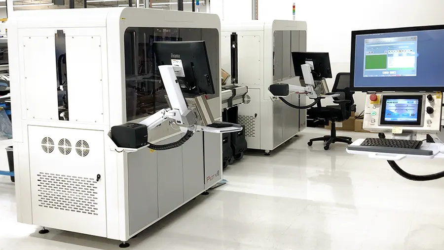
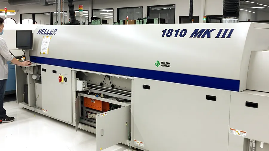
Our 70,000 sqft state-of-the-art campus in the heart of Silicon Valley contains the most advanced equipment required for the manufacture and assembly of your PCBs. Whether you’re looking for standard quick turn PCBs or boards with the tightest tolerances, made from exotic metals, there’s a reason Sierra Circuits leads the industry in quality and performance.

Get Started with RF/MW PCB Manufacturing and Assembly
We can turn your standard technology PCBs in as fast as in 24 hours.
Start a Custom Quote

Fabrication, Procurement, & Assembly. PCBs fully assembled in as fast as 5 days.
- Bundled together in an entirely-online process
- Reviewed and tested by Engineers
- DFA & DFM Checks on every order
- Shipped from Silicon Valley in as fast as 5 days

Fabrication. Procurement & Assembly optional. Flexible and transparent for advanced creators.
- Rigid PCBs, built to IPC-6012 Class 2 Specs
- 2 mil (0.002″) trace / space
- DFM Checks on every order
- 24-hour turn-times available

Complex technology, with a dedicated CAM Engineer. Stack-up assistance included.
- Complex PCB requirements
- Mil-Spec & Class 3 with HDI Features
- Blind & Buried Vias
- Flex & Rigid-Flex boards