Speak to an Account Manager
![]() +1 (800) 763-7503
+1 (800) 763-7503
Tools for Designers:
Impedance Calculator
Try This New ToolThe Sierra Circuits’ Impedance Calculator uses the 2D numerical solution of Maxwell’s equations for PCB transmission lines. It renders fairly accurate results suitable for use in circuit board manufacturing and engineering analysis.
In addition to the characteristic impedance of a transmission line, the tool also calculates:
- Signal losses that include total insertion, dielectric, and conductor losses
- Near-end and far-end crosstalk
- Capacitance
- Inductance
- Propagation delay per unit length
- Effective dielectric constant of the structure
- Coupling coefficient
- Even and odd mode characteristic parameters
Most of the free online impedance calculation tools are generally not accurate as they are based on empirical formulas and do not take into account the trace’s trapezoidal shape or the effect of multiple dielectric materials.
What is impedance?
The impedance between two points in an electronic circuit can be defined as the ratio of the voltage difference and the current. It is the AC voltage difference between the two points divided by the AC current. It is assumed here that the AC voltage and currents are sinusoidal with a frequency ‘f’ cycles/sec (the radian frequency, ω, equals 2πf radians/sec). In general, impedance is a function of frequency. The unit of impedance is Ohms (Ohm= volt/ampere).
- For a pure resistor of resistance R Ohms, the impedance ZR = R Ohms.
- For a pure inductor of inductance L Henries, the impedance ZL= jωL Ohms.
- For a pure capacitor of capacitance C Farads, the impedance ZC = 1/jωC Ohms.
- Impedances can be combined in series and parallel in the same manner as resistors.
Characteristic impedance of a transmission line
Signals propagate on a transmission line as electromagnetic waves with a propagation speed and attenuation factor per unit length. Between any point on the signal line and the corresponding point on the signal return path, the instantaneous AC voltage and the instantaneous AC current are related as follows:
Impedance of the transmission line at that point = (Instantaneous AC voltage)/(Instantaneous AC current)
This impedance is referred to as the characteristic impedance of the transmission line. If the transmission line has the same characteristic impedance along its length, it is called a uniform transmission line.
On a transmission line, whenever a propagating signal encounters a change in characteristics at any point, some part of the signal will be reflected, and signal distortion will occur. Therefore, to achieve good signal integrity, it is important to have a transmission line with uniform characteristic impedance.
Controlled impedance of a PCB transmission line
A PCB transmission line comprises a signal trace and its return path- usually the nearest reference plane(s). If the geometry of the signal trace, its return path, and the material between them is unchanged throughout the length of the trace, then we have a uniform PCB transmission line. A uniform transmission line will have the same characteristic impedance along its length. Taking into account the manufacturing considerations, achieving a reasonably uniform transmission line is termed a controlled impedance line, and its characteristic impedance is also referred to as controlled impedance.
When high-frequency signals propagate on transmission lines, uniform impedance is critical to achieving signal integrity, i.e., the transmission of the signal without distortion. Typically, you will need controlled impedance lines for high-speed digital and high-frequency RF/microwave applications.
Parameters required to calculate trace impedance
The impedance of circuit board traces is determined by:
- Trace width and thickness
- Height of the dielectric layer between the signal trace and the reference planes
- Dielectric constant(s) of the dielectric material used in the board
- Spacing between differential pair traces
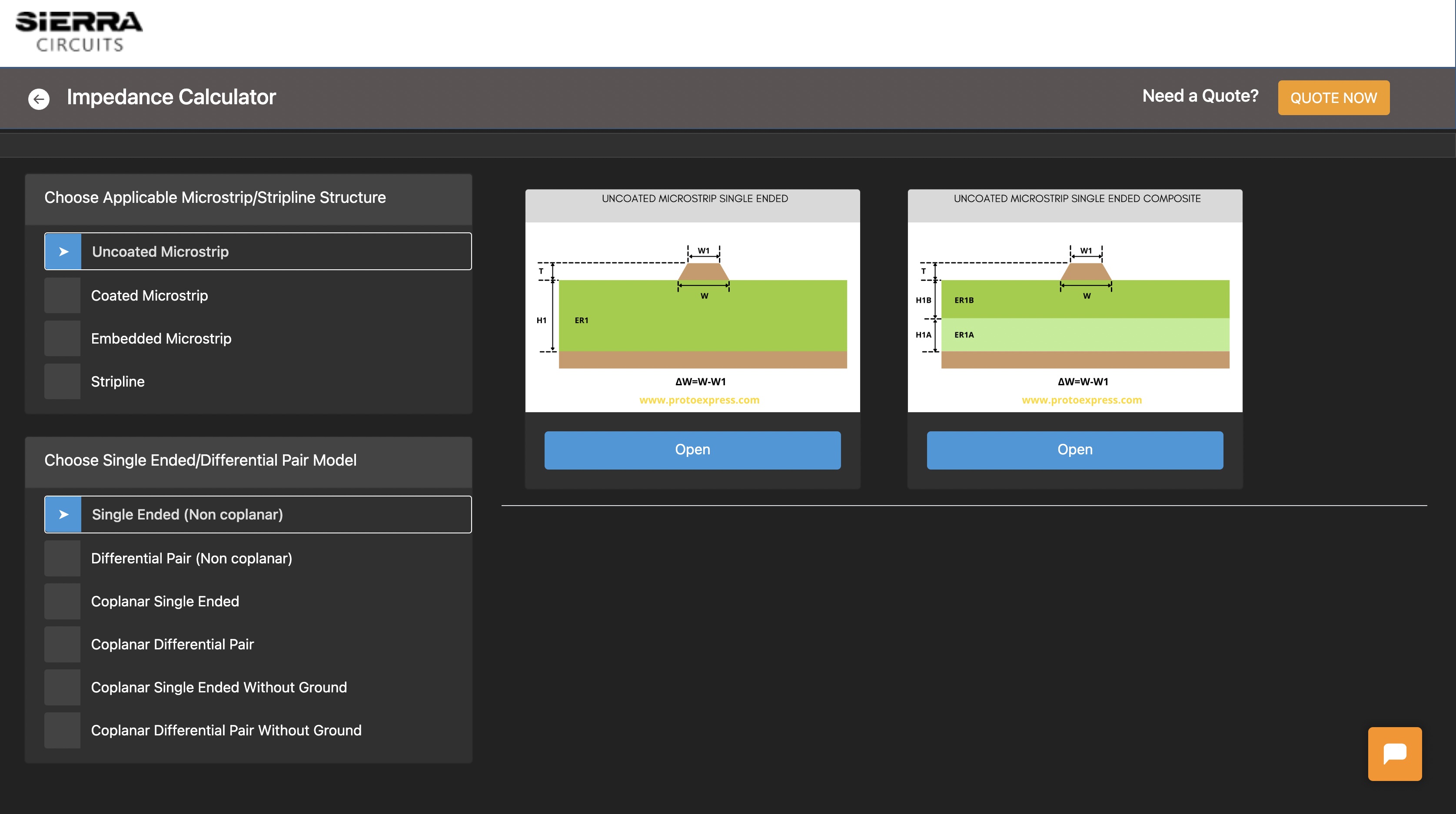
Types of impedance models
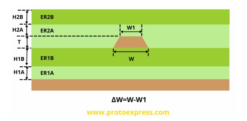
PCBs typically use two types of transmission line structures: microstrips and striplines. There are 3 types of microstrip models to choose from- uncoated, coated, and embedded. Each of the transmission lines consists of a signal trace and a reference plane(s). Within each model, the following combinations are available:
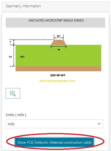
Uncoated microstrip single-ended
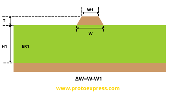
An uncoated microstrip structure consists of a signal trace on an outer layer of a PCB. The reference layer is typically the next layer above or below the signal layer trace. Uncoated microstrips do not have a soldermask coating above the trace.
Coated microstrip single-ended
A coated microstrip structure consists of a signal trace on an outer layer of a PCB. The reference layer is typically the next layer above or below the signal layer trace. Coated microstrips have a soldermask coating above the trace.
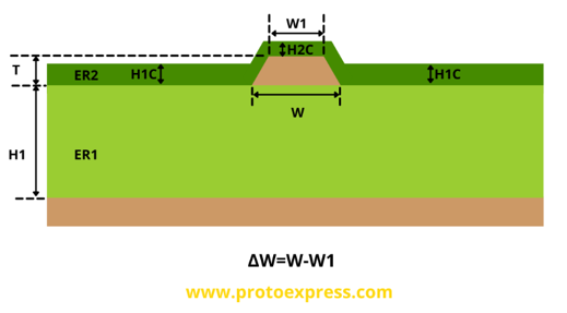
Embedded microstrip single-ended
An embedded microstrip is a structure similar to a traditional microstrip, except there is an extra dielectric layer above the signal trace. Embedded microstrips can be designed on the internal layers of a circuit board.
Stripline single-ended
A stripline is a structure composed of a uniform signal trace on an inner layer of a board. It is separated by a dielectric layer followed by copper planes on each side.
Our impedance calculator features two main types of impedance models, single-ended and differential, within each trace structure.
- There are 3 types of single-ended models: single-ended non-coplanar, coplanar single-ended, and coplanar single-ended without ground.
- There are also 3 types of differential models – differential, coplanar differential, and coplanar differential without ground.
List of our impedance calculators
Following is the table of 82 impedance calculators that are designed and categorized based on the different trace geometries:
Single-ended
| Uncoated | Coated | Embedded | Embedded (Inverted) | Stripline |
|---|---|---|---|---|
| Uncoated Microstrip Single Ended | Coated Microstrip Single Ended | Embedded Microstrip Single Ended | Embedded Microstrip (Inverted) Single Ended | Stripline Single Ended |
| Uncoated Microstrip Single Ended Composite | Coated Microstrip Single Ended Composite | Embedded Microstrip Single Ended Composite : A | Embedded Microstrip (Inverted) Single Ended Composite : A | Stripline Single Ended Composite : A |
| Embedded Microstrip Single Ended Composite : B | Embedded Microstrip (Inverted) Single Ended Composite : B | Stripline Single Ended Composite : B | ||
| Embedded Microstrip Single Ended Composite : C | Embedded Microstrip (Inverted) Single Ended Composite : C | Stripline Single Ended Composite : C |
Differential pair
| Uncoated | Coated | Embedded | Embedded (Inverted) | Stripline |
|---|---|---|---|---|
| Uncoated Microstrip Differential Pair | Coated Microstrip Differential Pair | Embedded Microstrip Differential Pair | Embedded Microstrip (Inverted) Differential Pair | Stripline Differential Pair |
| Uncoated Microstrip Differential Pair Composite | Coated Microstrip Differential Pair Composite | Embedded Microstrip Differential Pair Composite : A | Embedded Microstrip (Inverted) Differential Pair Composite : A | Stripline Differential Pair Composite : A |
| Embedded Microstrip Differential Pair Composite : B | Embedded Microstrip (Inverted) Differential Pair Composite : B | Stripline Differential Pair Composite : B | ||
| Embedded Microstrip Differential Pair Composite : C | Embedded Microstrip (Inverted) Differential Pair Composite : C | Stripline Differential Pair Composite : C | ||
| BroadSide Coupled Stripline Pair | ||||
| BroadSide Coupled Stripline Pair Over Core |
Coplanar single-ended
| Uncoated | Coated | Embedded | Embedded (Inverted) | Stripline |
|---|---|---|---|---|
| Coplanar Uncoated Microstrip Single Ended | Coplanar Coated Microstrip Single Ended | Coplanar Embedded Microstrip Single Ended | Coplanar Embedded Microstrip (Inverted) Single Ended | Coplanar Stripline Single Ended |
| Coplanar Uncoated Microstrip Single Ended Composite | Coplanar Coated Microstrip Single Ended Composite | Coplanar Embedded Microstrip Single Ended Composite : A | Coplanar Embedded Microstrip (Inverted) Single Ended Composite : A | Coplanar Stripline Single Ended Composite : A |
| Coplanar Embedded Microstrip Single Ended Composite : B | Coplanar Embedded Microstrip (Inverted) Single Ended Composite : B | Coplanar Stripline Single Ended Composite : B | ||
| Coplanar Embedded Microstrip Single Ended Composite : C | Coplanar Embedded Microstrip (Inverted) Single Ended Composite : C | Coplanar Stripline Single Ended Composite : C |
Coplanar differential pair
| Uncoated | Coated | Embedded | Embedded (Inverted) | Stripline |
|---|---|---|---|---|
| Coplanar Uncoated Microstrip Differential Pair | Coplanar coated Microstrip Differential Pair | Coplanar Embedded Microstrip Differential Pair | Coplanar Embedded Microstrip (Inverted) Differential Pair | Coplanar Stripline Differential Pair |
| Coplanar Uncoated Microstrip Differential Pair Composite | Coplanar Coated Microstrip Differential Pair Composite | Coplanar Embedded Microstrip Differential Pair Composite : A | Coplanar Embedded Microstrip (Inverted) Differential Pair Composite : A | Coplanar Stripline Differential Pair Composite : A |
| Coplanar Embedded Microstrip Differential Pair Composite : B | Coplanar Embedded Microstrip (Inverted) Differential Pair Composite : B | Coplanar Stripline Differential Pair Composite : B | ||
| Coplanar Embedded Microstrip Differential Pair Composite : C | Coplanar Embedded Microstrip (Inverted) Differential Pair Composite : C | Coplanar Stripline Differential Pair Composite : C |
Coplanar single-ended without ground plane
| Uncoated | Coated | Embedded | Embedded (Inverted) | Stripline |
|---|---|---|---|---|
| Coplanar Uncoated Microstrip Single Ended Without Ground Plane | Coplanar Coated Microstrip Single-Ended Without Ground Plane | Coplanar Embedded Microstrip Single-Ended Without Ground Plane | ||
| Coplanar Uncoated Microstrip Single-Ended Without Ground Plane Composite | Coplanar Coated Microstrip Single-Ended Without Ground Plane Composite | Coplanar Embedded Microstrip Single Ended Without Ground Plane Composite : A | ||
| Coplanar Embedded Microstrip Single Ended Without Ground Plane Composite : B | ||||
| Coplanar Embedded Microstrip Single Ended Without Ground Plane Composite : C |
Coplanar differential pair without ground plane
| Uncoated | Coated | Embedded | Embedded (Inverted) | Stripline |
|---|---|---|---|---|
| Coplanar Uncoated Microstrip Differential Pair Without Ground Plane | Coplanar Coated Microstrip Differential Pair Without Ground Plane | Coplanar Embedded Microstrip Differential Pair Without Ground Plane | ||
| Coplanar Uncoated Microstrip Differential Pair Without Ground Plane Composite | Coplanar Coated Microstrip Differential Pair Without Ground Plane Composite | Coplanar Embedded Microstrip Differential Pair Without Ground Plane Composite : A | ||
| Coplanar Embedded Microstrip Differential Pair Without Ground Plane Composite : B | ||||
| Coplanar Embedded Microstrip Differential Pair Without Ground Plane Composite : C |
Features of Impedance Calculator
- Allows you to choose the right impedance calculator mode based on the geometry of the signal layer and the relevant reference plane(s). Whether the traces are embedded in between layers or on the surface of the circuit board, you can easily choose the right type of calculator to suit your design needs.
- If you know the target impedance, the trace width can be calculated immediately. Similarly, If you have a target trace width, the impedance can be computed in a go.
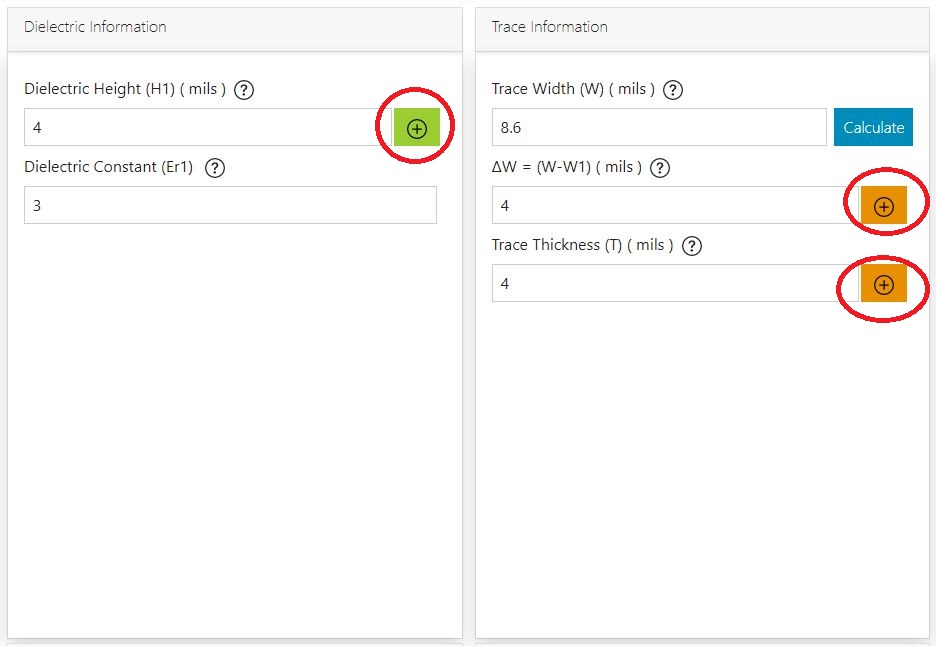
- The tool is integrated with a dielectric material construction table, which helps you fetch all the required dielectric information to perform the calculation.
- Input parameters such as dielectric thickness, Δw, and trace thickness can be updated just by clicking the respective plus button.
- Determines total insertion, dielectric, and conductor losses. These values are calculated based on the dissipation factor of the dielectric material, the frequency of the signal, surface roughness, and the length of the trace.
- Supports composite PCB models that use different dielectric materials to achieve the desired impedance. These models have been earmarked as ‘A,’ ‘B,’ and ‘C.’
- Composite model A: In this model, we have used two different dielectric materials at the bottom.
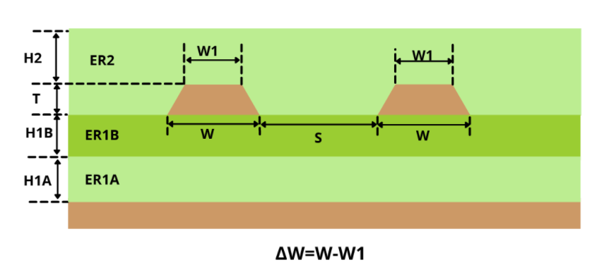
-
- Composite model B: Here, you can find two different dielectric materials on the top.
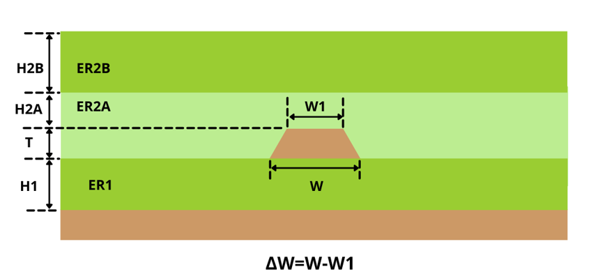
-
- Composite model C: In model ‘C’, two different dielectric materials can be found both on the top and bottom.
These composite models are also available for single-ended, differential pair, and coplanar configurations.
Benefits of composite PCB models
The dielectric that is closer to the trace has more effect on the trace’s impedance than the dielectrics that are afar. Composite geometry is most useful when multiple dielectric layers are present with different dielectric constants (Er). Instead of calculating effective dielectric constant, composite models allow us to use the parameters as it is to get more accurate impedance values. So, composite models are more practical in obtaining precise impedances than their non-composite counterparts.
How to use the tool
The Impedance Calculator evaluates single-ended and differential impedance for various impedance models. The tool also calculates signal losses of any given trace.
Calculation of impedance and trace width
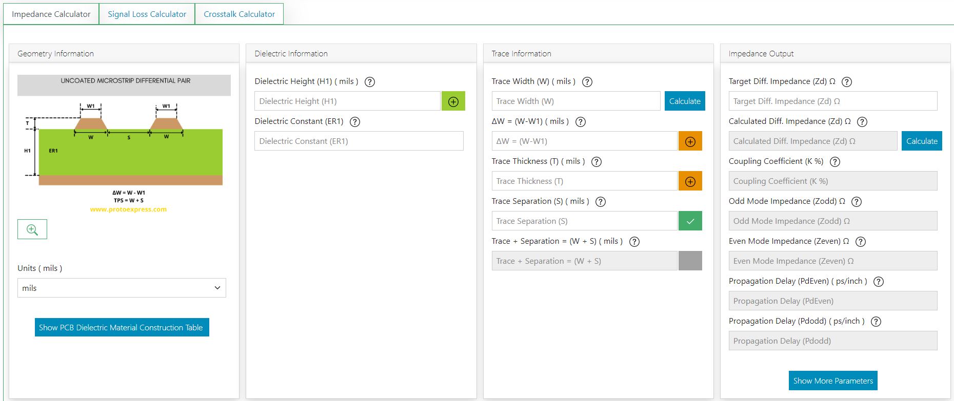
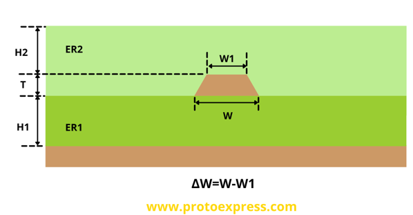
After selecting the relevant impedance model, you’ll have to key in the input parameters. For instance, if you select uncoated microstrip single-ended, the input parameters are:
Dielectric information:
- Dielectric height (H1)
- Dielectric constant (Er1)
Trace information:
- Trace width (W)/Targeted impedance
- Δw (W-W1)
The table below helps you to choose the right Δw value for different copper weights. It also provides the minimum trace width for the inner and outer layers.
| Copper weight Vs ΔW guidelines |
|||
|---|---|---|---|
| Copper weight | ΔW (W - W1) | Minimum trace width inner layer | Minimum trace width outer layer |
| ¼ oz | 0.5 mils | 2.5 mils | 3 mils |
| ½ oz | 0.5 mils | 3 mils | 4 mils |
| 1 oz | 1 mil | 4 mils | 6 mils |
| 2 oz | 3 mils | 6 mils | 8 mils |
| 3 oz | 6 mils | 8 mils | 12 mils |
| 4 oz | 7 mils | 9 mils | 14 mils |
- Trace thickness (T)
Once all the input parameters are entered, hit calculate to view the results.
The output parameters are:
- Target SE impedance/Trace width
- Calculated SE impedance
- Propagation delay
- Inductance
- Capacitance
- Effective dielectric constant
Please note that the input parameters might change depending on the impedance model you choose.
If you require any assistance with the Dk and Df value of the material, click on Show PCB Dielectric Material Construction table. This table shows the Dk and Df of the selected material for different thicknesses and resin content.
If you’d like to update the dielectric height and the corresponding dielectric constant, click on the plus button next to THE dielectric height.
Here, you can choose the dielectric height based on PCB type, board frequency, material, material type, and material thickness.
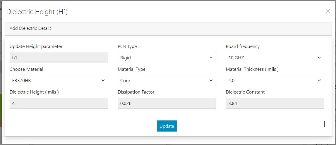
If you click on update, the dielectric height, dielectric constant, and dissipation factor will be automatically updated in the input section of the tool. Similarly, you can update the values of Δw and trace thickness using the respective plus buttons. After making these changes, click on the calculate button adjacent to the trace width field to view the new results.
If you have a specific trace width in mind, you can input that value and click on the calculate button beside the Calculated SE Impedance field to know the impedance of your trace.
The image below shows the output for the following input values:
- Dielectric height (H1) mils: 3.348
- Dielectric constant (ER1): 3.63
- ΔW: 0.5 mil
- Trace thickness: 1.45 mil
- Target impedance: 50Ω
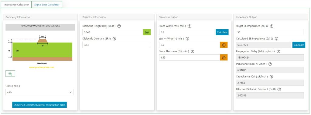
The units (mils, inch, mm, cm, μm) can be changed as per your requirement.
Computing signal loss of an impedance model
To calculate the signal loss for the chosen impedance model, you need to click on the Signal Loss Calculator tab. Please note that signal loss calculations use the dielectric and trace information entered in the impedance calculator. You won’t be able to compute signal losses without performing an impedance calculation.
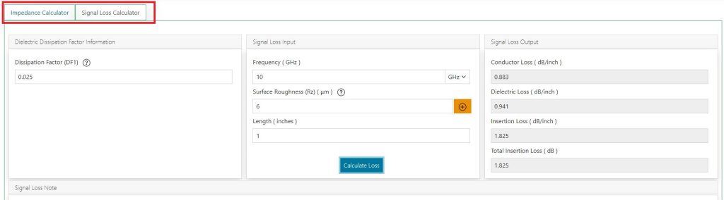
The input parameters are:
- Dissipation factor
- Frequency of the signal
- Surface roughness of copper foil
- Length of the trace
As mentioned earlier, the input parameters are subject to change depending on the chosen impedance structure.
Once all the input parameters are entered, click on Calculate Loss.
Now, let’s enter the dissipation factor as 0.025, the frequency as 10 GHz, the surface roughness as 6 μm, and the length of the trace as 1 inch.
The values of conductor loss, dielectric loss, insertion loss, and total insertion loss will be displayed as shown in the image above. If you require additional information on any of these input/output parameters, click on the corresponding help button.
How to calculate near-end and far-end crosstalk
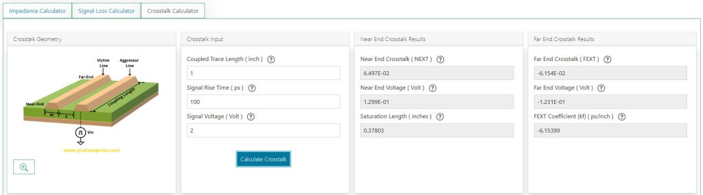
Based on the measurement zone, crosstalk can be classified into:
- Near-end crosstalk (NEXT): Noise on the driver end of the victim line
- Far-end crosstalk (FEXT): Noise on the receiver side of the victim line
To calculate them for your design, you need to provide the values of:
- Coupled trace length
- Signal rise time
- Signal voltage
Let’s enter the values as 1 inch, 100 picoseconds, and 2 volts for these parameters, respectively, and hit calculate crosstalk.
The tool displays the values of:
- Near and far-end crosstalk
- Near and far-end voltage
- Saturation length in inches
- FEXT co-efficient
Designing an appropriate impedance model to route your high-speed traces is essential to avoid signal distortion. This Impedance Calculator will give you the right impedance values based on your dielectric and conductor attributes.
Watch the demo of our Impedance Calculator

Sierra Circuits has developed easy-to-use tools for PCB designers and Electrical Engineers at every stage of circuit board development.


Fabrication, Procurement, & Assembly. PCBs fully assembled in as fast as 5 days.
- Bundled together in an entirely-online process
- Reviewed and tested by Engineers
- DFA & DFM Checks on every order
- Shipped from Silicon Valley in as fast as 5 days

Fabrication. Procurement & Assembly optional. Flexible and transparent for advanced creators.
- Rigid PCBs, built to IPC-6012 Class 2 Specs
- 2 mil (0.002″) trace / space
- DFM Checks on every order
- 24-hour turn-times available

Complex technology, with a dedicated CAM Engineer. Stack-up assistance included.
- Complex PCB requirements
- Mil-Spec & Class 3 with HDI Features
- Blind & Buried Vias
- Flex & Rigid-Flex boards