Speak to an Account Manager
![]() +1 (800) 763-7503
+1 (800) 763-7503
Tools for Designers:
Better DFM
Check Your DesignSierra Circuits acknowledges the various issues that PCB designers face while implementing DFM checklists. We have removed any pain points and simplified the design for manufacturing implementation process by developing a highly reliable and advanced DFM tool.
What is Better DFM?
Better DFM is an online design tool that checks for manufacturability of an electronic circuit design. The primary objective of this tool is to simplify the product design while enhancing the functional performance of the electronic circuit, making it easier to manufacture. We also offer our customers the opportunity to customize specific design parameters, as per their requirements.
Our tool allows users to load their IPC-356 format netlist along with Gerber files. This tool will create a netlist and compare it with the IPC netlist. Any errors (shorts or broken nets) in the design are identified in the report.
How does Better DFM help PCB designers?
Sierra Circuits’ PCB DFM tool is aimed at simplifying your design and manufacturing process by cross-verifying board design and parameters to save expensive corrections later on. Here are a few ways the tool will help you:
- Save time and money by identifying your PCB design errors ahead of time and prevent on-holds and re-spins.
- Get an instant price quote and place an order online.
- Ensure you have a complete set of files for manufacturing and electrically match your CAD design.
How to use the PCB DFM tool
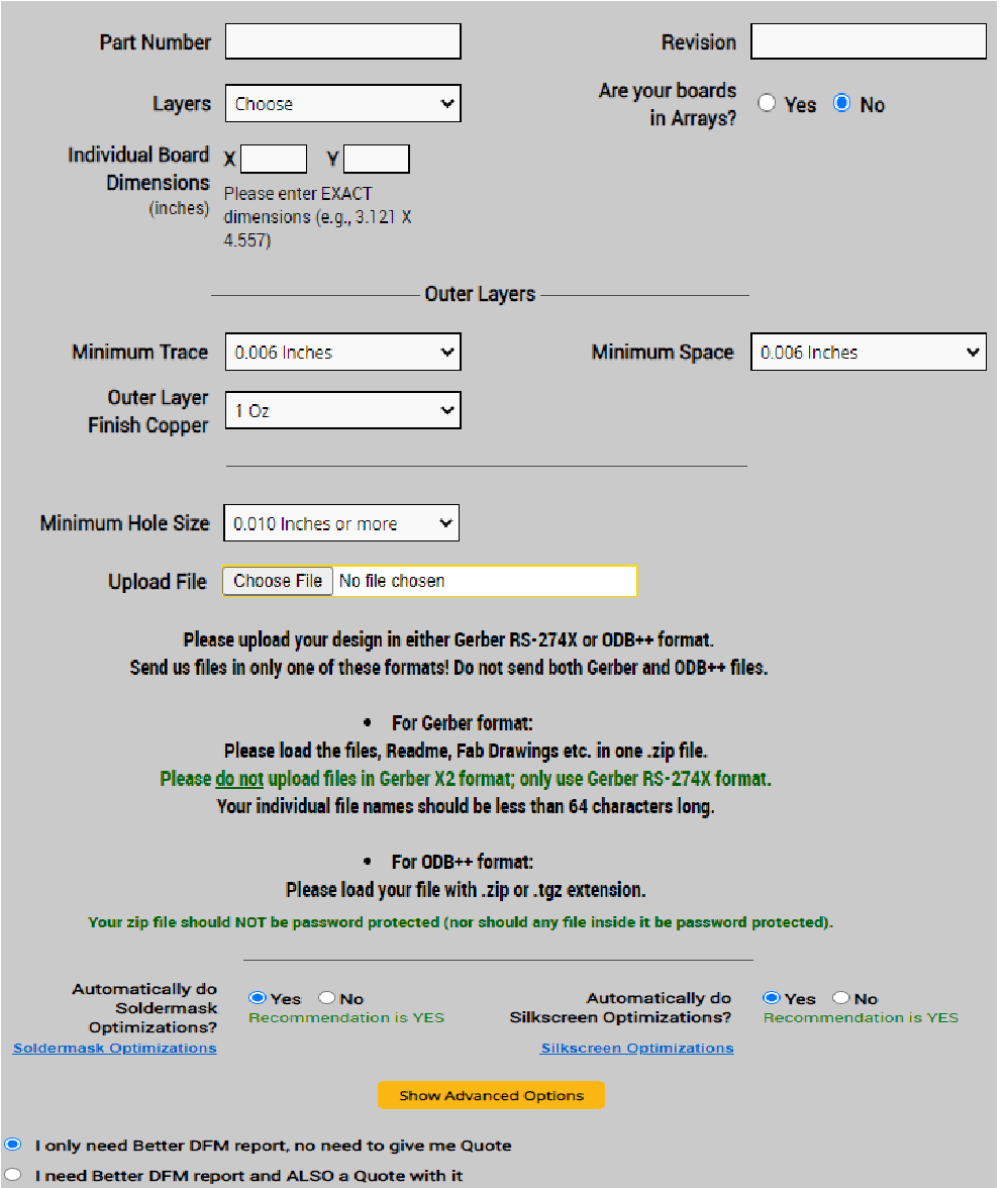
This image shows the interface of our Better PCB DFM tool. By providing the required information, users can get their DFM report sent by email. The tool has various sections for users to key in the data.
Here are the steps to validate your design using Better DFM:
1. Input your data
In the first section of the PCB DFM tool, you need to key in the part number (name of the design), revision (edition of the design), number of layers on the board and board dimensions. If your boards are to be manufactured in arrays, click on the option “Yes”.
If you choose to have the boards in an array, then the number of boards per array and the array dimension (in inches) should be provided.
In the next section, enter the following information related to outer layers.
- Minimum trace: It is the minimum conductor width in your design.
- Minimum space: It is the minimum space or air gap in your design.
- Outer layer finish copper: It is the thickness of the outer copper layer in ounces.
All the values in this section should be chosen as per your board specs.
After providing the outer layer information, you can define the minimum hole size using the drop down list.
2. Upload your Gerber files
The next step is to upload your files. You can do so by using the option “Choose File”
The following points should be kept in mind before uploading your files.
- Upload your design in either Gerber RS-274X or ODB++ format.
- For Gerber format, please, load the files, readme, fab drawings, etc. in one .zip file.
- Please, do not upload the files in Gerber X2 format; always use Gerber RS-274X format.
- Your individual file names should be less than 64 characters.
- For ODB++ format, upload your file with .zip or .tgz extension.
- Any of your files (including zip file) should not be password protected.
3. Automated solder mask/silkscreen optimizations
Once your files are uploaded, you can either opt for automated solder mask and silkscreen optimizations or decide against it.
Why should you opt for solder mask optimization?
If solder mask optimization is chosen, the Better PCB DFM tool will increase or decrease the solder mask clearances as needed for maintaining the required space (dam or bridge) between the clearances and copper coverage.
Our current manufacturing requirements are 3-mil space and 3-mil coverage.
When the clearances are much bigger than the pad, as in the case of pick-and-place fiducials, they are not decreased but may be clipped to maintain coverage when needed. If the clearances are smaller than the pads, they will not get increased. So, if your intent is to have masks on pads, they will not get affected.
In case optimization is not possible, and minimum manufacturing requirements cannot be met, we will show such locations in our DFM report for you to either fix the problems or let us know how to proceed.
Why should you opt for silkscreen optimization?
If the silkscreen optimization is opted, our Better DFM tool will clip the silk screen 3 mils away from the solder mask wherever overlapping or 3 mils away from the pads and holes where the solder mask is not available.
4. Advanced options
In the Show Advanced Options, you can define the minimum annular ring and minimum drill-to-copper requirements.
The basic definitions and explanations of annular ring and drill-to-copper can be accessed by clicking on the hyperlinks right below the drop-down lists.
This completes your input for our Better DFM tool if you are only looking for the design for manufacturing report. If you would like to receive a quote along with the report, then you need to provide a little more information. This is discussed later in this section.
After choosing the required option, click “Run Better DFM”. Once this is done, the layer assignment screen pops up as shown below. Here, you need to assign a file type for each of the Gerber files. Please, note that the layer assignment is only done for the layers which have a magnifying glass icon next to them. Once the layer assignment is completed, click the “Sort Layers” button.
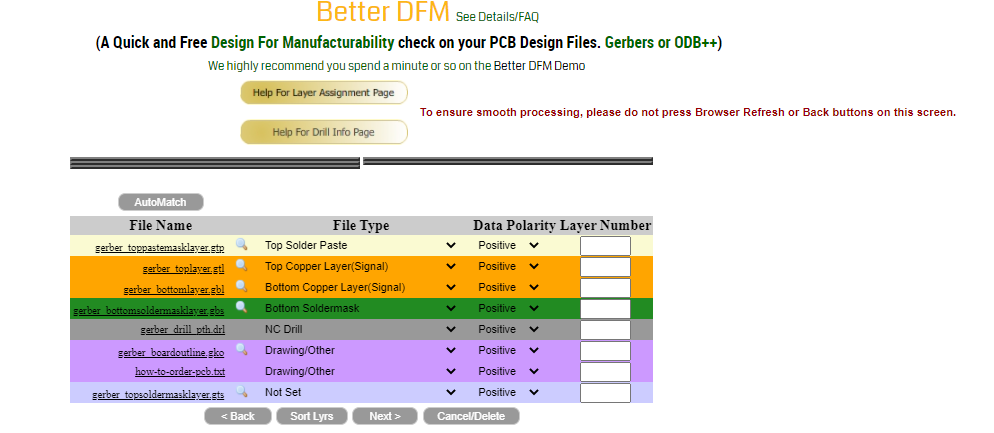
After sorting the layers, click the “Next” button. This will lead to the drill information page.
The drill information page ensures that correct drill sizes and plating types are provided in the drill file. After verifying the drill information, you need to click the “Submit” button. Now, the tool acknowledges that the upload is complete.
5. Get your design for manufacturability report
If there are no issues found in the uploaded files, you will receive an email stating that “No issues were discovered after running a DFM based on your input parameters. Therefore no design for manufacturing report was created.” If the tool discovers issues, you will receive an email.
By clicking “A DFM Report”, you can view the issues identified by the tool.
If you want a quote along with the report, select the option “I need Better DFM report and also a quote with it.”
Please, note that these instant web quotes are only available for simple standard technology boards. For instance, we cannot instantly quote PCBs with multiple laminations, or less than 0.005″ trace/space, or more than 10 layers. However, you can definitely run the Better DFM on even the most complex PCBs.
Better DFM 40-point checklist
The Better DFM does a comprehensive design for manufacturing analysis on your files.
Our 40-point checklist includes the following checks:
| Signal checks | Plane checks | Solder mask checks | Silkscreen checks | Drill checks |
| Conductor width | Drill-to-copper | Solder mask clearance | Silkscreen to mask spacing | Hole size |
| Spacing | Annular ring | Coverage | Silkscreen to copper spacing | Duplicate holes |
| Annular ring | Spacing | Rout to mask | Silkscreen to hole spacing | Hole spacing |
| Drill-to-copper | Conductor width | Spacing | Silkscreen to rout spacing | Touching holes |
| Hole registration | Thermal air gap / spoke width | Missing solder mask clearance | Line width | Plane shorts |
| Text features | Missing copper | Exposed lines | Text height | Holes to rout |
| Missing copper | Rout to copper | Partial clearance | Silkscreen over copper text | Missing holes |
| Features connection | Drill registration | |||
| Missing holes | Clearance smaller than the hole | |||
| Unconnected lines | ||||
| Rout to copper |
Better DFM reports
This PCB DFM tool provides the following reports:
- Report 1. DFM report (provided if we detect any issues in your Gerbers)
- Report 2. Netlist compare report (provided only if we find opens and shorts in your files)
- Report 3. Gerber layers shown in PDF format
Why is the Better DFM better?
- Sierra Circuits’ Better DFM is flexible and accurate. Along with checking against core manufacturability rules, it also allows you to put in your specific design rules to check against. You tell us what rules you are following and we’ll check against that.
For example, for an annular ring, you can specify if you want the Better DFM to test against tangency or breakout or some minimum width that is specified for the annular ring.
- We provide a full netlist comparison. If you load your IPC-356 format netlist with your files, we will create a netlist from your Gerber files and compare it with your IPC netlist. If there are any shorts and opens, we will show you which nets they are on.
- We provide a precise analysis in our DFM, with the exact location of features and real graphics.
- We can accept multiple drill files, and you can indicate which holes are plated or non-plated, and which layers they go through.
- For each layer in your Gerber files, the Better DFM gives you a PDF file showing that layer matched up against the drill holes, so you can spot any alignment issues.
- The Better DFM is hooked up to our popular PCB online service. So (if you choose) you can ask for an INSTANT price quote, and get some of the best value PCB pricing out there.
- If you choose to order PCBs, it is a cinch. Just pull up your quote and place an order online. It takes less than a minute!
Sierra Circuits has developed easy-to-use tools for PCB Designers and Electrical Engineers at every stage of circuit board development.


Fabrication, Procurement, & Assembly. PCBs fully assembled in as fast as 5 days.
- Bundled together in an entirely-online process
- Reviewed and tested by Engineers
- DFA & DFM Checks on every order
- Shipped from Silicon Valley in as fast as 5 days

Fabrication. Procurement & Assembly optional. Flexible and transparent for advanced creators.
- Rigid PCBs, built to IPC-6012 Class 2 Specs
- 2 mil (0.002″) trace / space
- DFM Checks on every order
- 24-hour turn-times available

Complex technology, with a dedicated CAM Engineer. Stack-up assistance included.
- Complex PCB requirements
- Mil-Spec & Class 3 with HDI Features
- Blind & Buried Vias
- Flex & Rigid-Flex boards