Embedded Components Design Guide
Sierra Circuits' Embedded Component Design Guide highlights how to select embedded passives and the benefits they offer over traditional SMDs.


Embedded Components Design Guide guide explains how to integrate embedded parts into the PCB to reduce parasitic effects and improve signal integrity.
Here’s a quick breakdown of what you’ll learn in this guide:
- Why embedded components are being adopted in high-density electronic systems
- How embedded passives minimize parasitic effects and improve high-frequency performance
- Key factors for selecting integrated resistors and capacitors
- Different embedded resistor technologies and their applications
- Material selection and stack-up design strategies for embedded components
- Best practices for integrating embedded passives into your PCB layout
- Techniques for achieving uniform impedance and effective decoupling
- Fabrication methods for embedded resistors and capacitors
- Guidelines for communicating embedded component requirements to your CM
The following sections will provide you with a closer look at each of these topics:
Why choose embedded components?
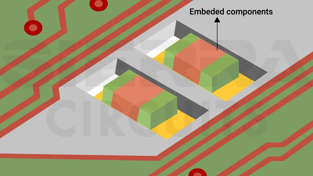
Surface-mounted passives consume valuable board real estate and introduce parasitic inductance and capacitance. Embedded components address these challenges by integrating passive elements directly within the PCB substrate. These parts enable thinner, lighter, and more compact products.
Integrated parts are beneficial in space-constrained applications such as smartphones, wearable devices, implantable medical electronics, and aerospace systems.
How do embedded components improve PCB performance?
Embedded components reduce the board form factor, minimize parasitic effects, and improve high-frequency behavior.
Here’s how they are beneficial:
Reduce form factor
One of the primary advantages of embedded passives is their ability to reduce the circuit board size.
By integrating passives within the board structure, you can save surface area for active components, connectors, sensors, and antennas. This makes embedded technologies suitable for compact prototypes.
Lower parasitic effects
Traditional surface-mount components introduce parasitic inductance and capacitance through pads, traces, vias, and solder joints.
These elements can negatively impact signal quality and power delivery, especially in high-speed designs. Embedded passives reduce interconnect lengths and place components closer to active circuitry. This helps minimize unwanted electrical effects and improve overall circuit performance.
Improve high-frequency behavior
As operating frequencies increase, maintaining signal integrity becomes more challenging. Embedded resistors and capacitors support high-frequency performance by reducing loop inductance, shortening current paths, and minimizing impedance discontinuities.
These characteristics make embedded passives useful in RF systems, high-speed digital designs, and applications that require improved noise suppression and stable signal transmission.
How to select the right integrated passives
Choosing embedded resistors and capacitors requires a clear understanding of their electrical, thermal, and mechanical characteristics. Integrated passives offer a limited range of values and may involve additional fabrication considerations.
Therefore, you must evaluate the required resistance or capacitance values, tolerances, power-handling capabilities, and frequency-response characteristics early in the design process.
For embedded resistors, factors such as target resistance range, tolerance, power rating, and temperature coefficient of resistance (TCR) determine whether the part can deliver stable performance under varying operating conditions.
Similarly, the effectiveness of embedded capacitors depends on capacitance range, tolerance, voltage rating, and high-frequency characteristics, including equivalent series resistance (ESR) and equivalent series inductance (ESL).
Carefully balancing these parameters with the application’s requirements will help you determine the most appropriate components and fabrication technologies.
What are the types of embedded resistors?
The Embedded Components Design Guide introduces different integrated resistor technologies and explains their trade-offs in cost, precision, and electrical performance.
The four most common types are printed, plated, thin-film, and thick-film resistors. They differ in the materials used, achievable tolerances, environmental stability, and suitability for high-frequency applications.
Understanding the characteristics of each technology helps you choose the most appropriate solution for your performance and manufacturing requirements.
Material selection and stack-up design strategies for embedded components
In the next chapters, the Embedded Components Design Guide explains how laminate selection and stack-up planning influence the performance and reliability of passives.
The performance and reliability of embedded components depend heavily on the materials used and how they are incorporated into the PCB stack-up. Selecting suitable resistive and capacitive laminates ensures stable electrical characteristics, thermal performance, and compatibility with fabrication processes such as etching and laser trimming.
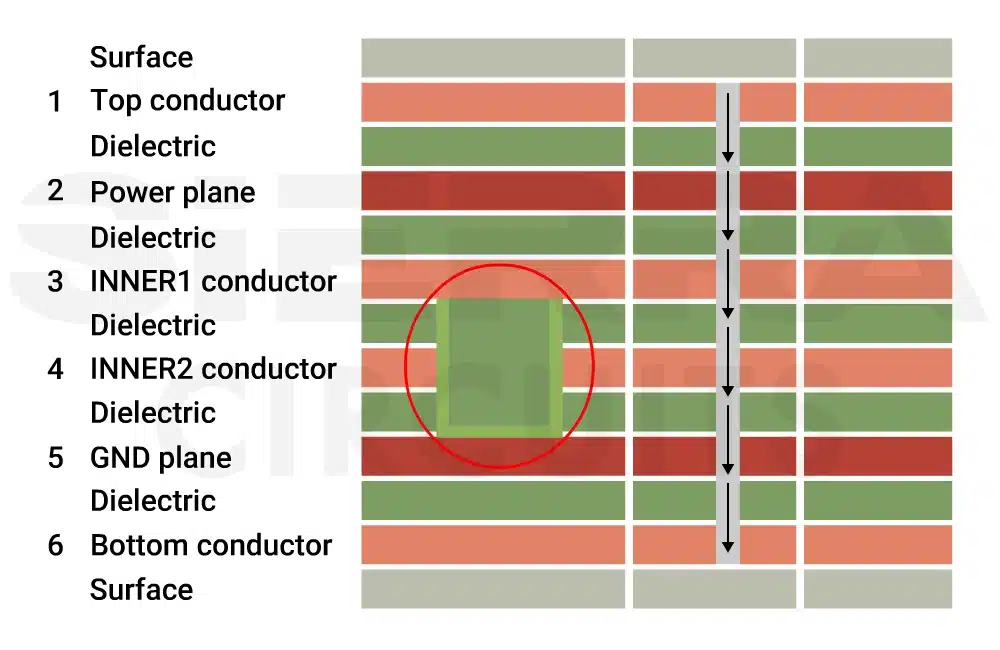
Designing a stack-up is equally important as it impacts both electrical performance and manufacturability. Embedded resistive and capacitive layers should be strategically positioned to minimize parasitic effects, improve decoupling, and maintain signal integrity.
You must also ensure stack-up symmetry, provide adequate clearances, and isolate embedded components from sensitive signal layers to avoid electromagnetic interference and simplify fabrication.
By carefully selecting materials and optimizing the stack-up, designers can maximize the benefits of embedded components while achieving reliable and manufacturable PCB designs.
How should you integrate embedded components into your layout?
The placement of embedded components significantly influences electrical performance. Embedded resistors and capacitors should be positioned as close as possible to the active devices they support, such as processors, memory devices, and power management ICs.
Shorter interconnect paths reduce trace resistance and parasitic inductance, enabling faster current delivery and minimizing signal degradation.
For example, placing embedded decoupling capacitors directly beneath a processor significantly reduces the current loop area between the capacitor and the device.
This lowers inductance and allows the capacitor to respond quickly to transient current demands. Similarly, termination resistors integrated near high-speed drivers and receivers help maintain signal quality by minimizing reflections and impedance discontinuities.
Routing considerations are equally important. You should provide dedicated paths between embedded components and the circuitry they serve to avoid unnecessary vias and long trace segments.
Excessive routing lengths can negate many of the performance advantages gained by embedding passive components within the PCB substrate.
The allocation of embedded components within the layer stack should also be planned carefully. Resistive layers and capacitive layers often serve different purposes and may require separate locations within the stack-up to simplify fabrication and testing. Proper layer assignment also helps avoid routing congestion and reduces interactions between embedded components and nearby signal layers.
How can you achieve uniform impedance with embedded passives?
Maintaining consistent impedance is one of the most important objectives in high-speed PCB design. Variations in impedance can lead to signal reflections, timing errors, and degraded signal quality. Embedded passives can contribute significantly to impedance control when they are implemented correctly.
Since embedded components shorten electrical paths and eliminate additional solder joints and mounting pads, they inherently reduce discontinuities that contribute to impedance variations. However, designers must still follow several practices to maintain uniform impedance throughout the design.
First, maintain consistent dielectric spacing between signal and reference planes. Variations in dielectric thickness directly affect transmission line impedance and can create impedance mismatches along critical routing paths.
Second, keep trace geometries uniform. Abrupt changes in trace width, routing direction, or reference plane configurations can introduce discontinuities that compromise signal integrity.
Third, place embedded resistive elements strategically within high-speed interconnects. Embedded termination resistors located close to transmitters or receivers can help absorb reflected energy and preserve signal quality.
The location of the capacitors also influences impedance characteristics. Embedded decaps positioned between power and ground planes create low-impedance current paths and suppress high-frequency noise. By minimizing loop inductance, they improve power integrity and help maintain stable impedance across a wide frequency range.
Shielding strategies are equally important. You should isolate embedded components from sensitive high-speed signals using ground planes or via stitching techniques. Proper isolation minimizes crosstalk and prevents EMI from affecting impedance-controlled circuits.
What are the best decoupling strategies with embedded capacitors?
In the upcoming chapters, the Embedded Component Design Guide covers best decoupling practices.
Power integrity has become increasingly important as devices operate at higher switching speeds and lower supply voltages. Conventional surface-mounted decoupling capacitors are often limited by parasitic inductance introduced by pads, solder joints, vias, and interconnecting traces. Embedded capacitors address these limitations by placing the energy storage elements much closer to the active circuitry.
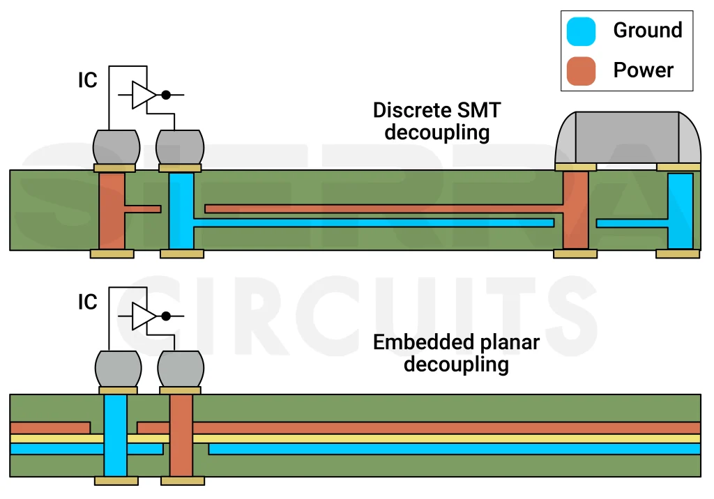
One of the most effective approaches is embedding low-value decoupling capacitors directly beneath high-speed devices such as processors, FPGAs, and ASICs. Their proximity to the power pins significantly reduces loop inductance and allows them to respond rapidly to transient current demands.
Embedded capacitors are particularly effective at suppressing high-frequency noise generated during device switching events. By creating shorter current return paths, they reduce voltage fluctuations and improve the stability of power distribution networks.
Another best practice is to position embedded capacitive layers between power and ground planes. This arrangement creates distributed planar capacitance throughout the PCB stack-up. The resulting low-impedance power delivery network provides additional high-frequency decoupling while improving electromagnetic compatibility.
However, embedded capacitors do not eliminate the need for conventional decoupling components in every application. In many practical designs, a hybrid strategy produces the best results. Low-value embedded capacitors can provide excellent high-frequency decoupling, while higher-value surface-mounted capacitors handle bulk energy storage requirements and lower-frequency transient loads.
This hybrid approach allows you to take advantage of the superior high-frequency characteristics of embedded capacitors without sacrificing flexibility in capacitance values and voltage ratings.
You should also carefully consider the electrical characteristics of the dielectric materials used to create embedded capacitors. Materials with low equivalent series resistance and low inductance provide better high-frequency performance and improve noise suppression capabilities.
Embedded capacitors provide a powerful mechanism for improving power integrity, reducing noise, and enhancing the electrical performance of high-speed electronic systems.
When combined with thoughtful placement, impedance control techniques, and optimized stack-up planning, they enable you to build compact, high-performance PCBs capable of meeting the demands of modern electronic applications.
How are embedded passives fabricated?
The fabrication of embedded passives involves integrating resistive and capacitive elements directly into the internal layers of a PCB.
Embedded passives require specialized materials and fabrication techniques to achieve the desired electrical characteristics while maintaining manufacturability and reliability.
Manufacturers commonly use additive and subtractive processes to produce integrated resistors.
Additive methods create resistive elements by depositing resistive materials onto the substrate through techniques such as screen printing or inkjet printing.
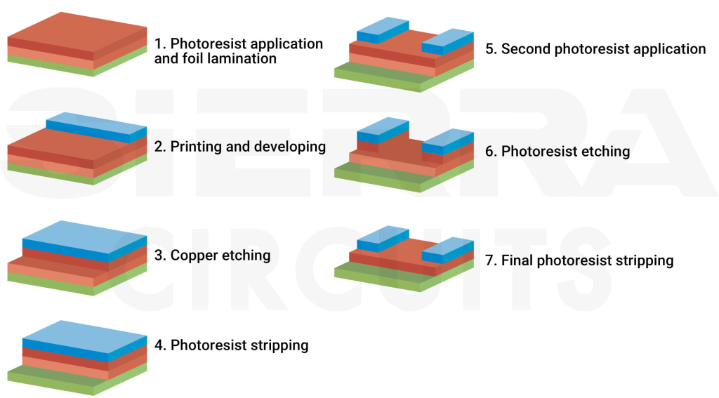
Subtractive methods use resistive foils, such as OhmegaPly and TCR materials, where the desired resistor patterns are formed through etching (as shown in the image above).
In applications that demand precise resistance values, laser trimming is often performed after fabrication to fine-tune the resistance.
Embedded capacitors are typically formed by laminating ultra-thin dielectric materials between power and ground planes to create distributed planar capacitance.
How should you communicate embedded component requirements to your manufacturer?
Successfully implementing embedded passives requires close collaboration between the PCB designer and fabricator. Since embedded components are integrated within the board structure, manufacturing requirements must be clearly documented early in the design cycle.
Fabrication notes should specify the type of embedded components, their target electrical values, tolerances, material requirements, and any special processing needs. You should also communicate requirements related to laser trimming, resistive or capacitive laminate selection, stack-up constraints, and testing expectations.
In addition, information about power handling, thermal considerations, and environmental requirements helps manufacturers select appropriate materials and processes.
Providing complete fabrication documentation reduces the risk of manufacturing errors, improves first-pass yield, and ensures that the embedded components achieve the intended electrical and reliability performance.
Early engagement with the manufacturer also helps identify fabrication limitations and enables design optimizations before production begins.
Download the Embedded Components Design Guide to learn practical techniques for integrating embedded passives, optimizing stack-ups, and improving signal and power integrity.