

Webinar: Material Selection for Reliable UHDI PCB Fabrication
REGISTER NOW
October 29th, 2026 | 9 AM PT
COST: FREE
-
10
Days
-
20
Hours
-
29
Minutes
-
33
Seconds
Amit Bahl
CRO at Sierra Circuits
Michael Gay
VP of Marketing at Advanced Chip & Circuit Materials
This webinar will be hosted on Zoom.
Following this event, you will receive:
-
 Slides
-
Recording
Webinar abstract:
Choosing UHDI technology to fit more components within a smaller form factor? Don’t focus solely on component placement and routing. The foundation of a successful ultra-HDI PCB lies in selecting the right materials.
Appropriate laminate helps you maintain precise layer alignment during multiple lamination cycles and ensure reliable interconnections at extremely fine geometries.
In this joint webinar with Advanced Chip and Circuit Materials, you’ll learn how to select UHDI PCB materials, design stack-ups, and apply DFM guidelines to ensure manufacturability.
Why material selection matters for ultra-HDI board fabrication
At 2-mil geometries, even minor material movement can compromise registration accuracy. Choose high-Tg laminates (>170°C) that can withstand repeated lamination cycles. Prioritize materials with a low Z-axis CTE (≤50-60 ppm/°C) to improve thermomechanical reliability.
Glass weave can also affect fine-line circuits by introducing impedance variations. Consider spread-glass weaves, such as 1067 and 1086, to minimize layer-to-layer registration errors.
REGISTER NOW
Beyond material selection, you must optimize your stack-up to maintain registration accuracy across multiple lamination cycles. Use a symmetrical stack-up and balance copper distribution across layers to minimize warpage.
You should also incorporate UHDI-specific DFM guidelines from the earliest stages of layout. Confirm your fabricator’s line and space capabilities, annular ring, and laser-drill diameter. Keep the total layer count to <16. For fine-line layers, incorporate 25 µm (1 mil) copper plating thickness.
Join this webinar to learn all about UHDI PCB materials and designing build-ups for fine-line PCBs.
Webinar agenda:
-
Why conventional materials may not meet UHDI requirements
-
Impact of material movement in layer-to-layer registration
-
Laminate behavior during laser drilling
-
Managing dimensional stability during multiple lamination cycles
-
Importance of CTE in ultra-HDI applications
-
Celeritas® materials for ultra-density boards
-
Impact of glass weaves and copper roughness
-
Stack-up considerations for minimizing registration errors
-
Plating challenges at 2-mil geometries
-
DFM guidelines for UHDI fabrication
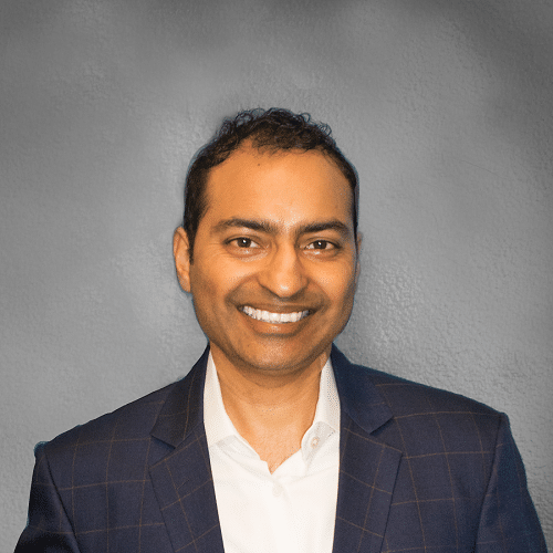
Amit Bahl, CRO at Sierra Circuits
Amit Bahl, widely recognized as the PCB Guy, currently serves as the Chief Revenue Officer at Sierra Circuits. He earned his Bachelor of Science in Engineering from UCLA in 1997, launching his career in Silicon Valley’s tech industry. In 2009, he assumed the role of Director of Sales and Marketing at Sierra Circuits, with a dedicated focus on democratizing design for manufacturing best practices and guidelines for PCB designers and engineers.
Within a short span, Amit successfully propelled Sierra Circuits to become a leading educational platform for all aspects of PCBs. Under his leadership, Sierra expanded to offer blogs, design guides, webinars, calculators and design tools, and a vibrant forum, SierraConnect. Amit remains committed to ensuring the community has access to the essential resources, whether they are developing standard products or boards with specifications for medtech or military applications.
Assuming the position of Chief Revenue Officer since 2022, Amit’s mission persists: to simplify the PCB design journey for all stakeholders. His unwavering dedication continues to drive Sierra Circuits as a trusted resource for the PCB design community.

Michael Gay, VP of Marketing at Advanced Chip & Circuit Materials
Michael J. Gay is Vice President, Marketing of Advanced Chip and Circuit Materials. Prior to his current role, he was Director High Performance Materials at Isola Group. Michael has been in the copper clad laminate and PCB manufacturing industries for 29 years.
As Director Emerging Products, Asia Pacific Region for Isola, based in Singapore, his responsibilities ranged from new product introduction, PCB process development, OEM collaboration and technical support and troubleshooting for industry customers. Since returning from his role in Asia, he has worked closely with major industry OEM’s to develop and qualify new materials for the next generation of technology. In his most recent position, he provided product application support and training, collaborative design support and design reviews for selecting rigid copper clad laminate materials across a wide range of applications including high speed digital, high energy/voltage, CAF resistance and RF/MW.
Michael is also active in various PCB industry organizations where he currently provides technical expertise to industry critical committees and projects and holds a Bachelor of Science in Mechanical Engineering and an MBA, both from Portland State University.



