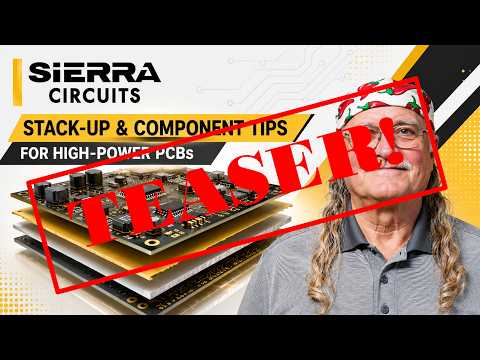
Stack-Up Design and Part Placement for High-Power PCBs

Daniel Beeker
President & CTO
System Solution Specialists

Vandana CC
Engineering Project Manager
Sierra Circuits
Fill out the form:
High-power electronic systems require carefully engineered circuit boards that can support large switching currents and stable power delivery. In applications such as DC-DC converters, motor drives, and industrial battery management systems (BMS), reliability is often determined less by the schematic and more by the stack-up and layout.
As switching frequencies rise and power densities increase, reference plane arrangement, dielectric spacing, and component placement directly influence parasitic inductance and EM field confinement.
In this webinar, you’ll learn practical tips to optimize these design factors, with a focus on high-power PCB stack-up design and part placement to improve signal integrity and overall reliability.
How to optimize stack-ups and component placement in high- power designs
You must consider copper weights and thermal resistance when designing circuit boards with high operating current. Standard multi-layer stack-ups with 1 oz copper are susceptible to thermal runaway and excessive IR drop when subjected to ≥30A current or rapid switching transients.
To prevent these failures, use heavier copper (≥2 oz) to carry high currents and reduce IR losses. Follow IPC-2152 standard charts to model your trace widths. Incorporate wide copper areas, thermal vias, and heat sinks to improve thermal dissipation.
A well-designed stack-up provides low-impedance power distribution with controlled return-current paths. Position power and ground planes on adjacent layers with thin dielectric spacing to suppress high-frequency noise.
The placement of power devices such as MOSFETs, gate drivers, and decoupling capacitors determines the size of current loops. Incorrect part placement might increase parasitic inductance. Therefore, keep current loops small and compact to minimize magnetic field radiation and voltage ringing. Position input capacitors close to switching devices to minimize voltage ringing.
To prevent unwanted capacitive and inductive coupling, separate switching MOSFETs, DC-DC converters, and motor drives from sensitive analog circuits. Implement grounded copper pours and multiple ground stitching vias (spaced at ≤ λ/20) around switching nodes to reduce radiated emissions.
What you’ll learn:
- Power-ground plane design
- Minimizing loop inductance
- Layer stack-up optimization
- Return current management
- Isolation between noisy and sensitive circuits
- Reducing EMI in switching converters and motor drives
- Thermal design considerations for high-power PCBs
- How to choose components for power electronics
- Q&A by Daniel Beeker
Presenters
Daniel Beeker, President & CTO of System Solution Specialists
With over 50 years of experience in electronic systems, Daniel Beeker currently serves as President and CTO at System Solution Specialists, providing expert PCB design review services with a focus on EMC, SI, and PI. By leveraging a science-based philosophy, Dan works to enhance design integrity across diverse market segments while collaborating with global clients to ensure reliable electronic designs.
Dan’s expertise spans advanced MCU and MPU application and tool design, as well as PCB analysis. Passionate about field-based design methodologies, he is committed to empowering teams and clients to achieve optimal performance and reliability in their electronic systems.
Vandana CC, Engineering Project Coordinator at Sierra Circuits
With a strong foundation in physics, Vandana CC brings a deep technical understanding to her work in PCB design and electronics manufacturing. She holds a Master’s in Physics and has experience teaching before transitioning into research at the Indian Institute of Science.
At Sierra Circuits, Vandana has played a key role in R&D projects, contributing to the development of engineering tools and calculators, technical content creation, and customer demos. Currently, she focuses on project coordination, ensuring seamless collaboration both within the team and with external partners. Her expertise bridges the gap between technical innovation and practical application, making her an integral part of Sierra Circuits’ engineering efforts.
Watch the Trailer