
Speak to an Account Manager
 +1 (800) 763-7503
mSAP Technology for Ultra-Fine PCB Trace and Space
Sierra Circuits specializes in mSAP technology to manufacture 2/2 mil line and space features with precise trace geometry and tight impedance tolerances.

How Does mSAP Enable Ultra-HDI Designs?
- Modified semi-additive process (mSAP) builds copper traces through an additive plating procedure rather than removing excess copper through etching (subtractive process). This approach helps to create ultra-fine features like 2 mil line and space technology with exceptional dimensional accuracy.
- They produce highly defined copper features with near-vertical sidewalls and minimal undercuts. This precise trace geometry helps maintain consistent impedance and signal performance.
- The resulting copper traces are smoother and uniform, reducing insertion loss and signal degradation, much needed in high-speed designs.
- Thinner traces and tighter spacing create more room for component pads, microvias, and other critical features, increasing circuit density without adding layers or increasing board size.
Ideal for:
- Ultra HDI applications
- Fine-pitch component routing
- Tight impedance requirements
- Dense RF and microwave layouts

Advanced mSAP Manufacturing Capabilities
- At Sierra Circuits, we have perfected the mSAP process to consistently manufacture ultra-HDI PCBs with trace and space features down to 2/2 mil (50/50 µm).
- We utilize SmartLam Dynachem laminator for uniform dry-film application and Nuvogo laser direct imaging (LDI) system for high-resolution patterning and superior registration accuracy.
- We accurately control photoresist exposure, curing, and electroless copper deposition to produce fully defined trace sidewalls and maintain critical feature integrity.
- We employ advanced plating and filling processes for laser-drilled microvias and stacked vias to create reliable interconnections in high-density designs.
- Our engineering team provides DFM analysis, stack-up optimization, and material selection recommendations tailored to your ultra-HDI and mSAP designs.
| Stack-Up | Stack-Up | ||
|---|---|---|---|
| Supported PCB Types | Rigid PCBs only (no flex) | ||
| Maximum Layer Count | 16 | ||
| Maximum Layers with 2/2 Technology | Up to 4 layers in the stack-up may utilize 2/2 technology | ||
| Maximum Copper Plating Thickness | 25 µm (1 mil) on layers containing 2/2 mil features | ||
| Maximum Overplating Tolerance | ±2 µm (0.079 mil) | ||
| Uniformity Across the Panel | ±10% | ||
| LDI Registration Tolerance | ≤±12 µm (0.472 mil) | ||
| Supported Materials | FR-4, Tachyon 100G, Panasonic Megtron 6, EM-528, and EM-892K | ||
| Unsupported Materials | Rogers | ||
| Maximum Board Size | 6"×6" | ||
| Trace and Space Clearance | Trace and Space Clearance | ||
|---|---|---|---|
| Minimum Trace/Space | 50/50 µm (2/2 mil) | ||
| Copper Thickness | 8–12 µm (0.31–0.47 mil) | ||
| Resist Thickness | 30 µm (1.18 mil) DI 9530 Dupont Dry Film | ||
| Plating Overgrowth Allowance | +5–8 µm (0.20–0.31 mil) per side | ||
| Artwork Compensation | −6 to −10 µm (−0.24 to −0.39 mil) | ||
| Minimum Trace-to-Via Pad | ≥60 µm (2.36 mil) | ||
| Minimum Trace-to-Copper Pour | ≥50 µm (1.97 mil) | ||
| Minimum Trace-to-Soldermask | ≥75 µm (2.95 mil) | ||
| Drill Parameters | Drill Parameters | ||
|---|---|---|---|
| Via Fill | Not supported on outer layers containing 2/2 mil features | ||
| Laser Via Plating Thickness | Up to 20 µm (0.8 mil) | ||
| Laser Via Diameter | 75–100 µm (2.95–3.94 mil) | ||
| Capture Pad | 100–125 µm (3.94–4.92 mil) | ||
| Minimum Annular Ring (IPC Class 2) | 25 µm (1 mil) | ||
| Minimum Mechanical Drill Size |
| ||
| Surface Finish | Surface Finish | ||
|---|---|---|---|
| Surface Finish Available |
| ||

Special DFM Guidelines for mSAP PCBs
- For multilayer designs, place 2/2 mil trace and space features only on the outer stack-up layers. Avoid routing ultra-fine features within thick core layers or buried structures.
- Avoid placing stacked microvias directly within 2/2 mil routing regions.
- Maintain balanced copper distribution throughout fine-line regions and avoid large copper voids to improve manufacturability and plating uniformity.
- Keep 2/2 mil circuitry away from panel edges to reduce the risk of fabrication defects and improve manufacturing yield.
- Consider the increased resistance of ultra-fine traces when routing long signal paths. For example, a 50 µm-wide, 10 µm-thick copper trace has an approximate resistance of 0.5-0.6 Ω/in.
- Reserve 2/2 mil traces for signal routing and avoid using them for power distribution.
- For high-speed RF, SerDes, and impedance-controlled designs, account for trace geometry, copper characteristics, and material properties during signal integrity analysis.
How to place an order for your mSAP PCBs

Trusted by innovators
Engineers at the worlds most innovative companies choose Sierra Circuits for the highest quality mSAP PCB manufacturing and assembly, right here in the USA.


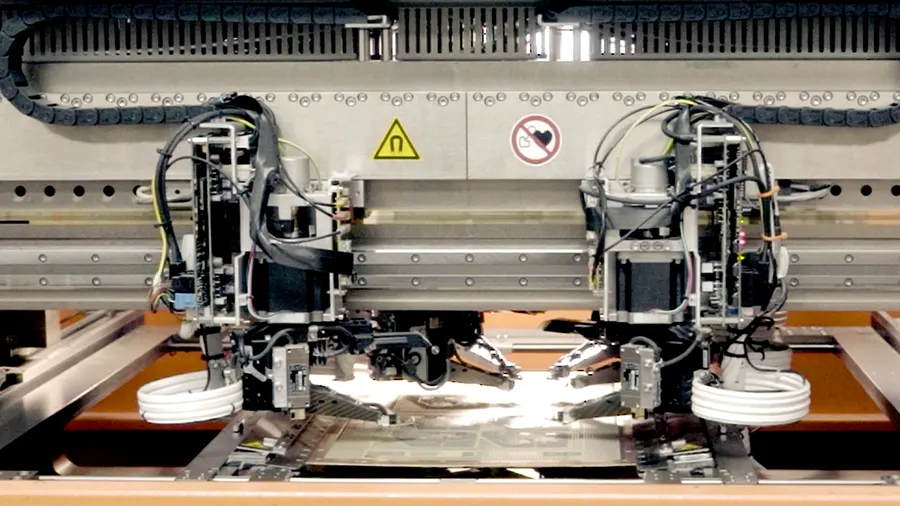
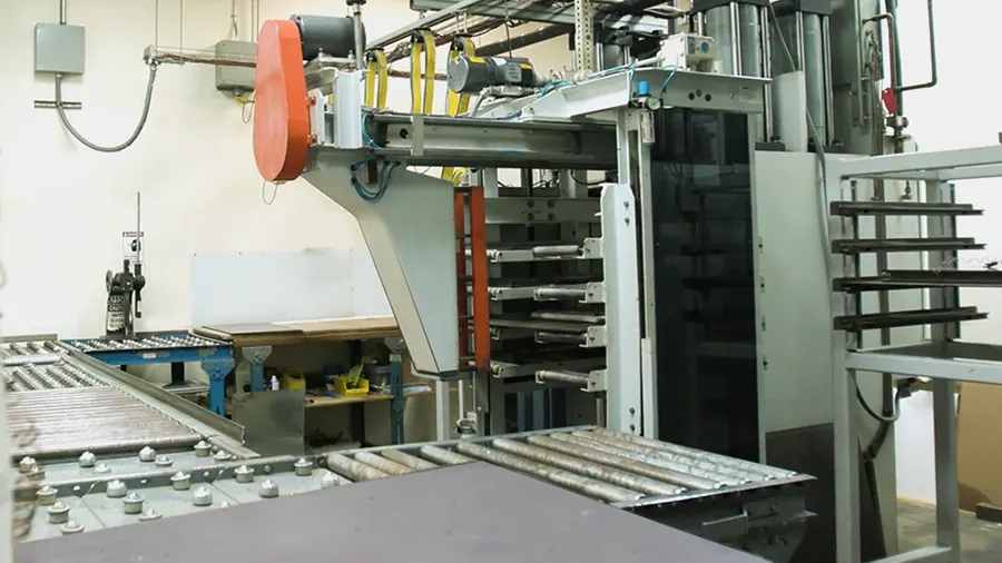

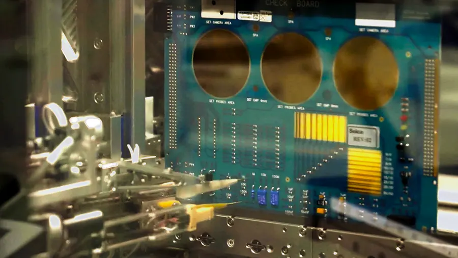
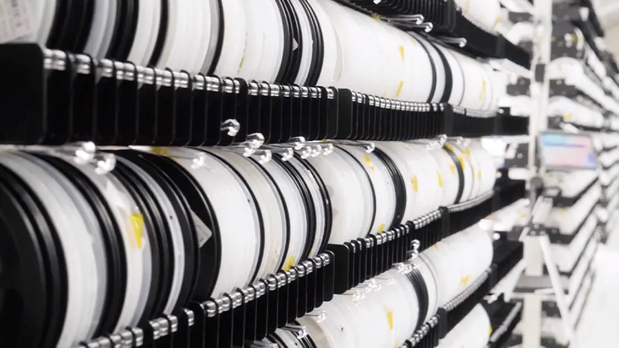

Manufacturing Equipment at Sierra Circuits
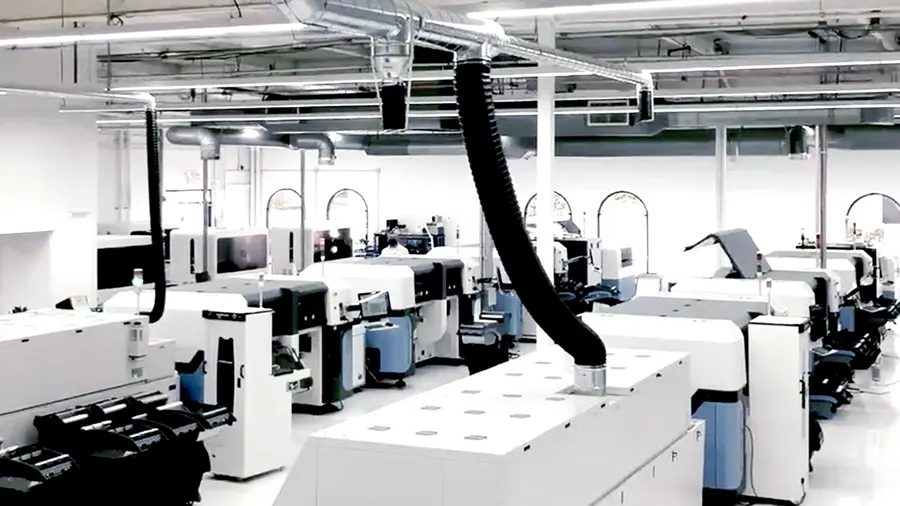
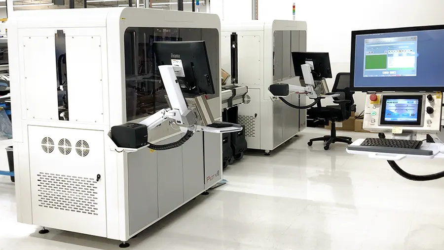
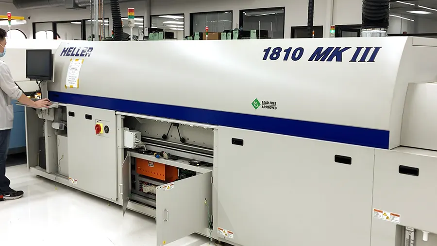
Our 70,000 sqft state-of-the-art campus in the heart of Silicon Valley contains the most advanced equipment required for the manufacture and assembly of your PCBs. Whether you’re looking for standard quick turn PCBs or boards with the tightest tolerances, made from exotic metals, there’s a reason Sierra Circuits leads the industry in quality and performance.



Fabrication, Procurement, & Assembly. PCBs fully assembled in as fast as 5 days.
- Bundled together in an entirely-online process
- Reviewed and tested by Engineers
- DFA & DFM Checks on every order
- Shipped from Silicon Valley in as fast as 5 days

Fabrication. Procurement & Assembly optional. Flexible and transparent for advanced creators.
- Rigid PCBs, built to IPC-6012 Class 2 Specs
- 2 mil (0.002″) trace / space
- DFM Checks on every order
- 24-hour turn-times available

Complex technology, with a dedicated CAM Engineer. Stack-up assistance included.
- Complex PCB requirements
- Mil-Spec & Class 3 with HDI Features
- Blind & Buried Vias
- Flex & Rigid-Flex boards