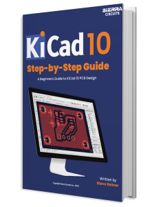
KiCad 10 Step-by-Step Guide
This KiCad tutorial walks you through the complete PCB design workflow, including schematic creation, layout design, and production file generation.


The KiCad 10 Step-by-Step Guide by Steve Kellner helps beginners learn the circuit board development process using the latest version of the EDA software.
What you’ll learn:
- Complete project workflow
- Creating symbol and footprint libraries
- Linking schematic symbols with their corresponding footprints
- Validating schematics using the electrical rules checker (ERC)
- Transferring schematic data into the PCB Editor and developing your layout
- Placing components and routing traces
- Running the design rules checker (DRC) to identify layout issues
- Generating production files
What is KiCad 10, and how do you design PCBs using it?
It is an open-source electronic design automation platform that helps you create schematics, assign footprints, design board layouts, test designs, and generate manufacturing files.
The typical workflow begins by creating a new project or opening an existing one. You then develop or populate symbol and footprint libraries and link the appropriate footprints to your schematic symbols. Once your libraries are ready, you can create the schematic and run the ERC to identify electrical issues.
After validating the schematic, you transfer the design to the PCB Editor, arrange your footprints, configure the board settings, define the board outline, and route the connections. You can then run the DRC to identify layout problems before generating the production files required to fabricate your printed board.
How to start a new project in KiCad?
Starting a project begins with creating an organized location for your design files. After launching the EDA tool, select File > New Project, choose the project location, and assign a name.
You can also open an existing project through File > Open Project when continuing a previous design.
Understanding how the tool organizes project files helps you manage your design files efficiently.
How to create and manage symbol and footprint libraries?
Symbol and footprint libraries provide the component information needed to develop your schematic and layout. A symbol represents the electrical function of a component, while a footprint defines its physical mounting pattern on the PCB.
KiCad 10 allows you to create custom libraries for the components used in your projects. You can populate symbol libraries with generic parts such as resistors and capacitors or add specific parts using their part numbers.
It lets you create custom footprint libraries and select footprints that match the physical components in your design. The guide recommends reviewing the 3D model of a footprint to verify if the land pattern matches the part.
After creating your libraries, you can link each symbol to its corresponding footprint. This connection ensures that the correct physical representation of each component is transferred to the layout.
Organizing your libraries and verifying footprints early in the design process can prevent potential errors in the development process.
What are the steps to create and validate a schematic in KiCad 10?
Once your component libraries are ready, you can create your schematic in the Schematic Editor. The process involves placing symbols, connecting their pins, and adding power and ground symbols where required.
The EDA tool uses PWR_FLAG symbols to identify power nets that are driven by a power source. Adding these symbols can resolve common ERC errors related to undriven power pins.
After completing the schematic, run the Electrical Rules Checker. The tool displays errors and warnings and highlights their locations in the schematic, allowing you to review and resolve problems before moving to board layout.
How to import the schematic into the layout?
After validating the schematic, you can use the Update PCB from Schematic option to transfer the design into the PCB Editor (layout). The tool captures the component footprints and the electrical connections between them.
After importing the footprints, you can arrange them as required. Next, define the board outline and start developing the physical layout.
The tool’s align/distribute option can help you organize components, while the ratsnest (thin lines between the footprints) provides a visual guide for planning connections.
Once placement is complete, you can route traces between component pads. The guide also explains how to manage circuit board layers and ensure that traces, text, and other design elements are placed on the correct layers.
When should you run ERC and DRC?
KiCad provides two important design verification tools: ERC for schematic validation and DRC for layout verification.
The electrical rules checker should be run after creating the schematic to identify electrical problems before the design moves to the PCB Editor.
After completing component placement and routing, run the Design Rules Checker to identify physical layout issues and rule violations. Review the reported errors and warnings, correct the problems that affect your design, and rerun the checker as needed.
Some warnings may be acceptable depending on your design, but you should evaluate each one rather than ignoring them automatically.
Using ERC and DRC as part of your regular workflow can help identify problems before your design reaches the fab house.
How to generate production files in KiCad 10?
You can use the Fabrication Outputs option to export Gerber/ODB++/IPC-2581 data.
The EDA tool allows you to create fab files that describe the different board layers, along with drill files containing information about the holes required in the board. You can also generate a bill of materials containing information about the components used in your design.
Before sending your design to a PCB manufacturer, organize the required production files and verify that they correspond to the final version of your board. The guide explains how to locate the generated files and package them for delivery to your fabricator.
Download the KiCad 10 Step-by-Step Guide to quickly learn the complete board design workflow and create production-ready designs with confidence.