Speak to an Account Manager
![]() +1 (800) 763-7503
+1 (800) 763-7503
Tools for Designers:
PCB Conductor Spacing and Voltage Calculator
Try This New ToolSierra Circuits PCB Conductor Spacing and Voltage Calculator computes the minimum spacing between two conductors if the potential difference between them is provided. Conversely, if the spacing between two conductors is given then the maximum potential difference that can be allowed between them is computed.
With this tool, you can get an accurate estimate of the space and voltage required between the conductors. This is particularly helpful during the PCB design and layout stages. The calculator is largely based on IPC 2221B standard, table 6-1.
What does the IPC 2221B standard convey?
The IPC 2221B standard describes the generic circuit board design requirements that include component mounting or interconnecting structures for single-layered, double-layered, or multilayered boards. All the design principles and calculations are carried out based on the regulations depicted in this standard.
Some of the important parameters mentioned in this standard are clearance, creepage, trace thickness, trace spacing, maximum applicable voltage, etc. The PCB Conductor Spacing and Voltage Calculator operates based on these principles.
How to get started with the tool
On the left of the tool page, you can select the type of conductor geometry required. The available configurations are:
- Conductors on internal layers
- External conductors uncoated
- External conductors uncoated (above 3050 meters)
- External conductors SM (solder mask) coated,
- External conductors with conformal coating
- Component leads uncoated
- Component leads with conformal coating
By default, it is set to conductors on internal layers. Each of these options is described below:
IPC 2221B electrical conductor spacing standards clearly distinguish between internal conductors, external conductors, and component leads. Therefore, these options give different values for the maximum voltage and minimum spacing requirements.
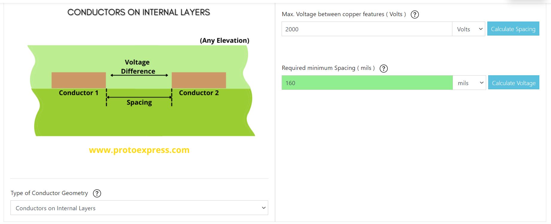
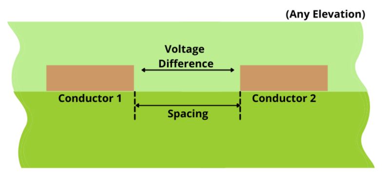
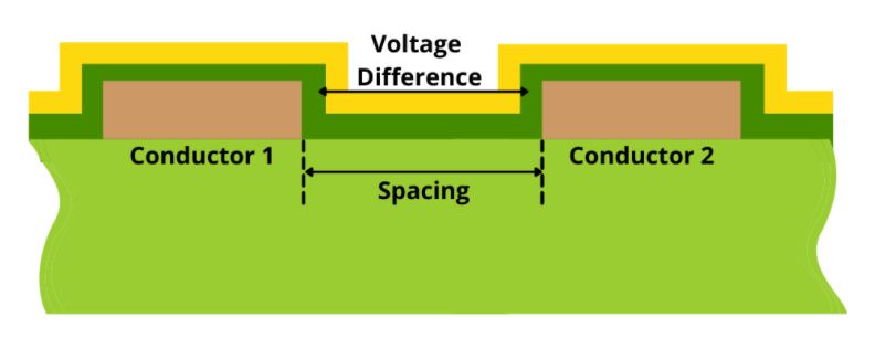
Conductors on internal layers
These conductors are present on any inner layer of the board stack-up.
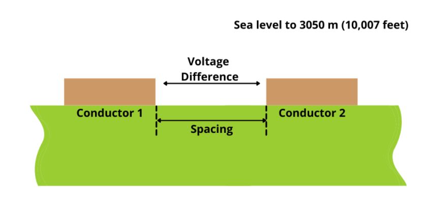
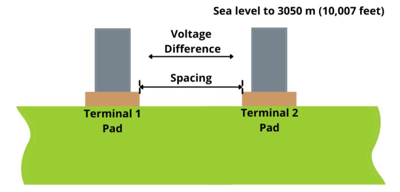
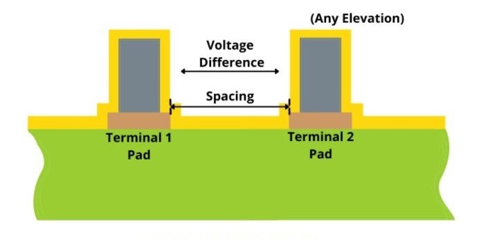
External conductors uncoated
This type of conductors are present on the external layers and are uncoated. This option has 2 variants – sea level to 3050m (10,007 feet) and above 3050m (above 10,007 feet). Both these options have different calculation values.
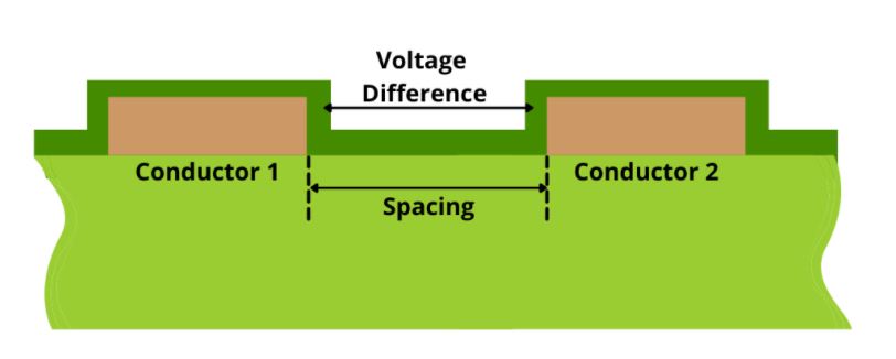
External conductors coated
These conductors are present on the external layer of the board and are coated. It has two geometries: solder mask coated and conformal coated.
Component leads
Component leads are also considered as conductors with spacing requirements between them. These leads or terminations can either be uncoated or conformal coated. Both geometries have different sets of requirements and calculations.
Calculation of maximum voltage or minimum spacing between conductors
On the right, maximum voltage between copper features and minimum spacing required for a particular voltage can be calculated. Drop downs beside these options can be used to select units.
Click on help option to know more about these parameters.
Now, if you would like to calculate the minimum spacing between traces for a specific voltage, input the voltage value and hit calculate spacing. This displays the minimum spacing for the given voltage. When the minimum spacing is known and the maximum voltage that can be applied needs to be calculated, the same procedure is followed.
Let’s calculate the minimum spacing required for a voltage of 2000V.
First, select conductors on internal layers as the type of geometry. Input 2000 in the maximum voltage between copper features and choose the units as volts. Now, hit calculate spacing to compute the required minimum spacing value. The tools shows that the required minimum spacing is 160 mils.
The PCB Conductor Spacing and Voltage Calculator is fairly simple to use and offers a user-friendly interface. You can follow the same procedure to calculate maximum voltage and minimum spacing for all the other trace geometries.
Watch the tool demo:

Sierra Circuits has developed easy-to-use tools for PCB designers and Electrical Engineers at every stage of circuit board development.


Fabrication, Procurement, & Assembly. PCBs fully assembled in as fast as 5 days.
- Bundled together in an entirely-online process
- Reviewed and tested by Engineers
- DFA & DFM Checks on every order
- Shipped from Silicon Valley in as fast as 5 days

Fabrication. Procurement & Assembly optional. Flexible and transparent for advanced creators.
- Rigid PCBs, built to IPC-6012 Class 2 Specs
- 2 mil (0.002″) trace / space
- DFM Checks on every order
- 24-hour turn-times available

Complex technology, with a dedicated CAM Engineer. Stack-up assistance included.
- Complex PCB requirements
- Mil-Spec & Class 3 with HDI Features
- Blind & Buried Vias
- Flex & Rigid-Flex boards