


Contents

Webinar: Dielectric Anisotropy Implications for Transmission Line Impedance and Via Modeling
by Bert Simonovich
May 2nd, 2024
10:00 am to 11:00 am PT
Accurately determining the impedance of the circuit requires you to incorporate the appropriate parasitic elements in your models, which can significantly influence the actual impedance value. Circuit simulation, online impedance calculator, and practical formula-based approach help you calculate the impedance of the circuit.
Understanding the impedance of a circuit is crucial for ensuring efficient signal flow and minimizing disruptions.

Impedance is an AC characteristic of a circuit that may vary with the operating frequency. It is normally represented by Z = R – j/ωC + jωL where ω= 2πf.
Highlights:
- You can calculate the impedance of a circuit through simulation tools, online calculators, and practical estimation methods.
- The impedance of your PCB mainly depends on material choice, stack-up configurations, transmission line impedance, power delivery network impedance, and via impedance.
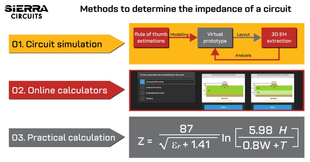
Methods to determine the impedance of a circuit
The impedance of a circuit can be calculated using the following methods.
1. Circuit simulation

Circuit simulation is a technique used to verify the functionality of a board design before manufacturing. Impedance calculation is now included in many PCB design software programs. One of the main advantages here is that the impedance design parameters can be modified to perform various simulations. Once the simulations are carried out, you can choose the best design to manufacture.
Here’s what Eric Bogatin, Professor Univ. of Colorado, ECEE, says about the most effective simulation tools on SierraConnect, “I use Ansys Electronic Desktop, Hyperlynx, ADS, and Polar simulation tools to predict high-frequency behavior .”
2. Online impedance calculators
Controlled impedance or trace parameters can be determined using online calculators. Although not as detailed as simulation tools, these can get you close enough to where only minimal adjustments by your CM are required for manufacturability.

Sierra Circuits Impedance Calculator employs a 2D numerical solution of Maxwell’s equations for PCB transmission lines. It produces data that are fairly accurate and suitable for circuit board manufacture. The tool estimates trace parameters such as capacitance, inductance, propagation delay per unit length, and the effective dielectric constant of the structure.
Unlike our impedance tool, most free online impedance calculators aren’t very accurate because they’re based on empirical formulas and don’t account for the trapezoidal shape of the trace or the effect of numerous dielectric materials.
3. Practical method
Follow the below steps to arrive at an approximate controlled impedance value quickly.
Calculate the rise time for the trace using the formula,
tr = 0.35 / fmax where fmax is the maximum operating frequency.
Now, calculate the maximum trace length,
l = tr x 2 in/ns
The characteristic impedance of the trace can be calculated using the below formula:

Where
- εr is the dielectric constant of the material (as per the datasheet)
- H is the height of the trace above ground
- W is the width of the trace
- T is the thickness of the trace
What is the difference between impedance and resistance?
The primary distinction between resistance and impedance is that resistance opposes both DC and AC current flow, whereas impedance opposes AC current. Impedance has no significance in a DC circuit.
Some of the key differences are tabulated below:
| Resistance | Impedance |
|---|---|
| Denoted by 'R'. | Denoted by 'Z'. |
| Unaffected by the supply frequency. | Mainly depends on supply frequency. |
| Two or more resistances in series can be added arithmetically. | Vector addition should be performed to sum up the impedances. |
| Current through resistance is always in phase with the voltage across it. | Current and voltage are out of phase. The phase difference depends on the inductance or capacitance present in the impedance. |
Why is impedance matching important in PCBs?
At high frequencies, board traces act as transmission lines with specific impedance values at each point. Impedance matching ensures that it remains constant at each point throughout the trace. Fluctuating impedance in a transmission line results in signal reflection, hampering the signal integrity. Controlled impedance ensures that signals are not degraded as they propagate through the trace.
If there is a change in impedance anywhere along the signal path, a portion of the signal is reflected to the source, resulting in a reduced signal at the load. These reflections can cause signal distortion, ringing of the signal, and potentially affect the functioning of the circuit.

The reflection coefficient (Γ) is given by (Zl-ZO) / (Zl+ZO)
The amount of reflection and its polarity can be calculated using the following equation.
Percentage of reflection = 100 * (Zl – ZO) / (Zl + ZO)
ZO is the impedance before the change, and Zl is the impedance after the change.
The reflection coefficient defines the degree of reflection in a transmission line. The value ranges from 0 to 1.
- Γ=0 indicates no reflection;
- Γ=1 indicates total reflection;
- 0<Γ<1, signifies partial reflection
Common locations where impedance variations occur on PCBs
Here’s an infographic that shows a few instances where impedance variations arise on a circuit board. Adhere to the guidelines given to avoid impedance discontinuity.

Factors affecting controlled impedance
The impedance of a trace is determined by the physical dimensions of the trace (trace width and thickness), dielectric constant, and distance to the reference plane (dielectric thickness) of the board material. It ranges between 25 and 125 Ohms. The following factors impact the impedance of PCBA:

Factors affecting the impedance of PCB trace
- Width (w) and thickness (T) of the copper signal trace (top and bottom)
- Thickness (H) of the core or prepreg material on either side of the copper trace
- Dielectric constant (εr) of the core and prepreg material
- Distance from other copper features
Controlled impedance is necessary for high-speed applications such as signal processors, telecommunication, and RF transmission.
What determines the overall impedance of a circuit board?
The impedance of a circuit is determined by the arrangement of the components. Resistors, capacitors, and inductors are some of the basic circuit elements. Resistors oppose the current flow, and the resistance value is independent of the supply frequency. On the other hand, capacitors and inductors offer reactance, a function of the frequency of the input signal.
In an ideal world, the capacitor should have reactance inversely proportional to the signal’s angular frequency. Inductors should offer reactance directly proportional to the signal’s angular frequency.
Apart from the parameters mentioned above, the impedance of a circuit depends on the PCB substrate and the inner conductive planes. The insulator, along with the interior layers, creates parasitic capacitance and inductance. These parasitic elements result in cross-talk and affect the overall impedance of the circuit. Now, we will see a few factors that influence the impedance of your circuit board.
Transmission line impedance

The impedance of a transmission line mainly depends on its characteristic impedance, which is essentially the impedance of a transmission line in total isolation. The other metrics that quantify transmission line impedance are even and odd mode impedances. Even and odd modes are the two basic signal propagation modes across a paired transmission line.
Odd mode impedes a transmission line when two traces in a pair are operated differentially (signals with the same amplitude and opposite polarity).
Even mode impedes a transmission line when two traces in a pair are operated evenly (signals with the same amplitude and direction).
Transmission line impedance also depends on how traces are arranged relative to each other. Two traces placed close to each other experience inductive and capacitive coupling. This coupling normally results in cross-talk and also changes the impedance on each line.
To understand how to reduce the impedance mismatch on a PCB trace, see how to limit impedance discontinuity and signal reflection in PCB transmission lines.
Controlled Impedance Design Guide
6 Chapters - 56 Pages - 60 Minute ReadWhat's Inside:
- Understanding why controlled impedance is necessary
- Stack-up design guidelines
- How to design for impedance
- Common mistakes to avoid
Download Now
Power delivery network impedance
At lower frequencies, the power delivery network will have capacitive impedance, lowering the resistance of the power bus that drives the components and current return path. The physical separation between power rails, traces, and internal planes defines PDN impedance. As the input frequency rises, so does the PDN impedance.

The impedance spectrum is useful for determining a bandwidth with the lowest power delivery network impedance. It should remain flat across the board’s operational range. To maintain the power integrity of the board, the placement of the ground plane is crucial.
When traveling toward the ground plane, signals will take the path with the least reactance. The path with the least reactance should be directly beneath the conductors on the board. This will ensure that the circuits have the least loop inductance and are less susceptible to EMI.
Board material selection and stack-up

PCB stack-up is an arrangement of board materials in sequential order. The image above depicts a 4-layer stack-up. L1 and L4 are the outer layers, and L2 and L3 are the inner layers.
As mentioned earlier, the neighboring conducting layers in a board build-up create a parasitic effect that impacts the overall impedance of the circuit. Impedance mismatch caused by parasitics will produce reflections on the trace, eventually introducing cross-talk and EMI issues.
Stack-up also acts as documentation that expresses your expectations to the manufacturers. A missing piece of information might make it difficult or impossible for fabricators to understand exactly what the requirements are.
To learn about effective documentation for controlled impedance, see specifying your controlled impedance requirements.
Choosing the right material that best suits the design is the key to avoiding these circumstances. Dielectric constant (Dk) affects the geometry of a trace with a specific impedance value. Resin content and material thickness are the two critical components that determine the Dk of a material. It decreases as the thickness increases. That means the higher the resin content, the lower the Dk value.
The below pointers will help you select the appropriate materials and avoid variations in overall impedance value.
- Determine the right layer thickness: Thinner layers reduce the loop area and parasitic inductance while increasing the parasitic capacitance. To find the appropriate layer thickness, you can use simulation tools with various layer stacks.
- Opt for material with a lower dielectric constant: Substrates with a higher Dk value produce more stray capacitance. Always choose a lower Dk substrate, especially for high-speed applications.
- Avoid choosing a very low resin content substrate: Very low resin content may lead to resin starvation, resulting in impedance variation.
- Do not use more than three types of prepregs in a stack-up: Having different prepregs can be risky as it increases the chance of a greater variation in the final thickness. If several prepregs are used, the effective dielectric constant of the composite material should be calculated using the weighted average method.

High-Speed PCB Design Guide
8 Chapters - 115 Pages - 150 Minute ReadWhat's Inside:
- Explanations of signal integrity issues
- Understanding transmission lines and controlled impedance
- Selection process of high-speed PCB materials
- High-speed layout guidelines
Download Now
Via impedance
Vias and through holes in a multilayer board will have parasitics between neighboring conductive elements. The inductance of a via will be in the order of nano henries and is mostly determined by its aspect ratio.
The via impedance is generally around 25 to 35 Ohms. Hence, there is a significant difference between the impedances of vias and traces (around 50 ohms). When a via hole is placed on conductive traces, noise coupling causes impedance discontinuities. Always avoid placing vias between the differential pairs to reduce the discontinuities.
Regardless of how you determine the impedance of the circuit board, you should collaborate with your contract manufacturer (CM), as DFM standards and material availability will affect the production of your board. In the comments section, let us know if you need assistance with your controlled impedance design. We would be happy to help you. Check our controlled impedance capabilities to learn more about our services.

Key Takeaways:
- Impedance is critical in PCB design, influencing signal quality and power delivery.
- Impedance changes can lead to signal distortion, ringing, and potential circuit malfunction.
- PCB trace impedance depends on trace width, thickness, dielectric constant, and distance to the reference plane.
- The overall impedance of a circuit board is influenced by component arrangement and parasitic elements.
- Material selection, stack-up arrangements, dielectric constant, resin content, material thickness, transmission line impedance, power delivery network impedance, and via impedance influence impedance control.
- Collaboration with contract manufacturers and adherence to DFM standards is essential for successful impedance control.
Need assistance in designing your circuit board schematic? Post your questions on SierraConnect and get them answered by industry experts.


Start the discussion at sierraconnect.protoexpress.com