


Contents

Webinar: Dielectric Anisotropy Implications for Transmission Line Impedance and Via Modeling
by Bert Simonovich
May 2nd, 2024
10:00 am to 11:00 am PT
Annular rings are one of the biggest concerns of PCB designers. You know that you may place your via right in the middle of the pad in the design files, but it just does not mean that you will 100 percent avoid tangencies, or even worse, breakouts. Let’s talk about annular rings, shall we?
What is an annular ring?
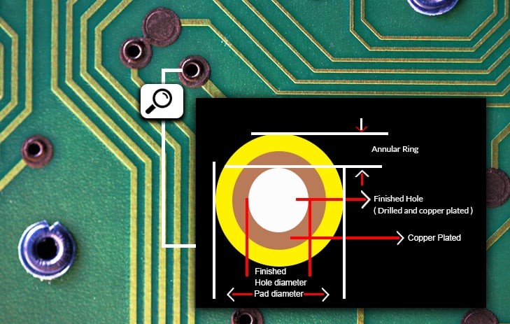
An annular ring is the area of copper pad around a drilled and finished hole. The finished hole we are talking about here is nothing but a copper-plated via. All around this via there should be enough copper to form a solid connection between the copper traces and the via in a multi-layer PCB. Therefore, the main purpose of an annular ring is to establish a good connection between a via and the copper trace.
Annular ring provides an area for connecting leads or wires to the electronic component, which serves as an anchor for the circuit. The minimum diameter will be determined by the manufacturer’s PCB assembly capabilities which can vary based on the nature of the holes and whether or not they are plated.
Construction of an annular ring
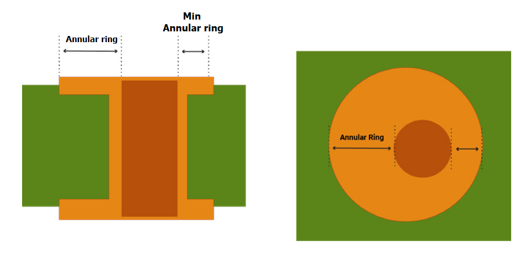
When you need to connect traces to another layer in a multi-layered board, you typically have to place a copper pad on your circuit board and drill a via on it to make the connection. The outer ring surrounding the via after the drilling process constitutes the annular ring.
How do you calculate the annular size?
Ideally, designers want their annular rings with holes located dead-center in order to get the best connection possible between the vias and the layers.
The perfect width is the difference between the diameter of the copper pad and the diameter of the finished hole divided by two.
- Annular ring width = (Diameter of the pad – Diameter of the finished hole) / 2
For example, if your pad diameter equals 22 mils and the hole diameter equals 10 mils, then the width is calculated in this manner: (22 – 10) / 2 = 6 mils.
Why does the ring size matter?
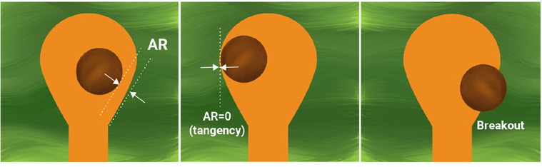
The width of the ring should be sufficiently thick to allow reliable electrical connection with via. The minimum length of the ring should be greater than or equal to the specified width for the design. A dimension that is less than the value specified in the design can interfere with the attachment of the component. It can also lead to pad breakout (zero annular ring), a condition associated with the region where the circuit enters the pad. This can reduce the current-carrying capacity of the circuit.

Common annular ring issues
- Undesired annular ring
- Tangency
- Breakout
All the above may arise due to insufficient ring width in the design.
Annular ring and vias
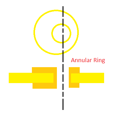
The via hole must be drilled at the absolute center of the pad to form the annular ring or the minimum width of the ring must be above the specified value. Misregistration of the via with respect to the land can lead to marginal interconnections that exhibit increased resistance and perhaps lead to reliability problems.
The graph below displays the probability of breakout plotted vs the annular ring.
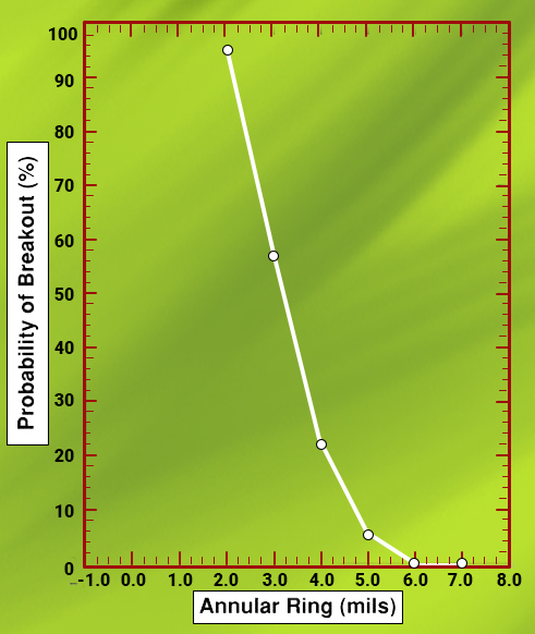
The smallest clearance (−1 mil), included to verify that the proper hole size was drilled, is intentionally designed to fail. The probability of breakout decreases from 98 percent for the 2 mils designed clearance to zero for the 6 and 7 mil clearances. If the breakout is not allowed, then designs fabricated by the supplier in this example would require rings of 6 mils or larger for the microvias. By designing 5 mil annular rings, the data estimate that 5 percent of the microvias will exhibit breakout.
What is teardrop pad?
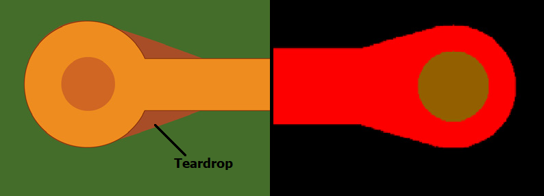
The name “teardrop” is because of its shape. Teardrop pad is an extra feature that adds additional copper at the junction of annular rings with PCB traces. This shape can increase the structural integrity against mechanical or thermal stress.
During the drilling process, there is a possibility of misalignment of the drill bit which removes too much copper from the junctions of a via pad and PCB trace causing the possibility for a broken trace connection or too thin of a connection. In such cases, a teardrop shape can increase the manufacturer’s tolerance of drill in the pad which can help reduce the rejection count in the production.
The importance of using teardrop increases as the traces become narrow. Teardrop rings are not necessary for conductors bigger than 20 mils. Also, teardrops are recommended for flex PCBs because of its structural integrity against shear and vibration.
Annular ring plays a critical role in PCB design and manufacturing. Hence, it’s a good practice to make sure all your annular rings are carefully crafted.
To know more about flex PCBs check out our article Rigid-Flex Cuts Electronic Product Assembly Costs
How Sierra can help you
Designing for manufacturing is the key to success. The free Better DFM is an online tool that checks your Design For Manufacturability. When using this tool, you have the possibility to go to Advanced Options and choose what you need to check for in your annular rings. You now have several options:

IPC Class 3 Design Guide
8 Chapters - 23 Pages - 35 Minute ReadWhat's Inside:
- IPC guidelines for manufacturing defects
- IPC standards for assembly processes
- Common differences between the classes
- IPC documents to set the level of acceptance criteria
Download Now
- Tangency is the default option. If you are willing to accept tangency on pads in your manufactured board, the Better DFM will look for a minimum of 5 mils (0.005″) annular ring width in your design.
- When you need to have a minimum 1 mils ring on pads in your manufactured board, then the Better DFM will look for a minimum of 6 mils (0.006″) annular width in your design.
- If you are targeting a ring of minimum 2 mils on pads in your manufactured board, the tool will look for a minimum of 7 mils (0.007″) ring width in your design.
- Lastly, if you do not mind having breakouts on pads in the manufactured board, the Better DFM will practically not look for any minimum ring width in your design. However, this option is not recommended.
The Better DFM does not only check for annular rings. The tool does a comprehensive Design For Manufacturability (DFM) analysis on your files.

The Better DFM 40-point checklist includes the following DFM checks:
Signal Checks
Plane Checks
|
Solder Mask Checks
Silk Screen Checks
|
Drill Checks
|

Design for Manufacturing Handbook
10 Chapters - 40 Pages - 45 Minute ReadWhat's Inside:
- Annular rings: avoid drill breakouts
- Vias: optimize your design
- Trace width and space: follow the best practices
- Solder mask and silkscreen: get the must-knows
Download Now


