Speak to an Account Manager
![]() +1 (800) 763-7503
+1 (800) 763-7503
Related Categories — HDI / Blind & Buried Vias » PCB Design » Signal Integrity
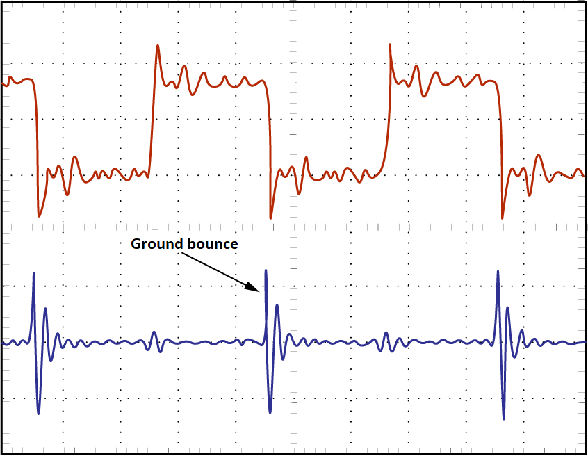
How to Reduce Ground Bounce in PCB Assembly
Ground bounce is a source of noise in a PCB assembly. It is important to prevent this as it interrupts high-speed or high-frequency operation. The major cause for ground bounce is the difference in ground potentials at various points on the circuit.
PCB Assembly
Decoupling Capacitor Placement Guidelines for PCB Design
Decoupling is a way of isolating signal components from composite signals based on frequency. Therefore, understanding which range ... more »
PCB Assembly
How to Reduce Signal Attenuation in High-Speed PCBs
Signal attenuation is the most prevalent term when high-speed signals propagate on a circuit board. It is one ... more »
High Speed
How to Reduce Ground Bounce in PCB Assembly
Ground bounce is a source of noise in a PCB assembly. It is important to prevent this as ... more »
PCB Assembly
Decoupling Capacitor Placement Guidelines for PCB Design
Decoupling is a way of isolating signal components from composite signals based on frequency. Therefore, understanding which range ... more »
PCB Assembly
How to Reduce Signal Attenuation in High-Speed PCBs
Signal attenuation is the most prevalent term when high-speed signals propagate on a circuit board. It is one ... more »
High Speed
Unlock Your Signal Integrity Analysis Potential
Signal integrity analysis provides the measurement of the amount of signal degradation when the signal travels from the ... more »
PCB Design
Losses in PCB Transmission Lines
A PCB transmission line comprises at least two conductors – one for the signal and another for its ... more »
PCB Design
How to Handle Current Return Path for Better Signal Integrity
Before we start with today’s article, something needs to get engraved in your mind. If some current goes ... more »
PCB Design
How to Avoid Crosstalk in HDI Substrates?
Miniaturization of the copper features in electronic circuits results from placing interconnections closely with a high packing density. ... more »
HDI / Blind & Buried Vias
The Effects of High-Speed Signals in a PCB Design
The designers are constantly challenged to improve the performance of an electronic product. At the same time, the ... more »
High Speed
9 Factors That Lead to Signal Integrity Issues in a PCB
Avoiding signal integrity issues in a PCB is an extremely complex task for designers. It requires a deep ... more »
Controlled Impedance


Fabrication, Procurement, & Assembly. PCBs fully assembled in as fast as 5 days.
- Bundled together in an entirely-online process
- Reviewed and tested by Engineers
- DFA & DFM Checks on every order
- Shipped from Silicon Valley in as fast as 5 days

Fabrication. Procurement & Assembly optional. Flexible and transparent for advanced creators.
- Rigid PCBs, built to IPC-6012 Class 2 Specs
- 2 mil (0.002″) trace / space
- DFM Checks on every order
- 24-hour turn-times available

Complex technology, with a dedicated CAM Engineer. Stack-up assistance included.
- Complex PCB requirements
- Mil-Spec & Class 3 with HDI Features
- Blind & Buried Vias
- Flex & Rigid-Flex boards