Speak to an Account Manager
![]() +1 (800) 763-7503
+1 (800) 763-7503
Related Categories — HDI / Blind & Buried Vias » PCB Design » PCB Manufacturing » Via
How to Choose the Right HDI PCB Materials
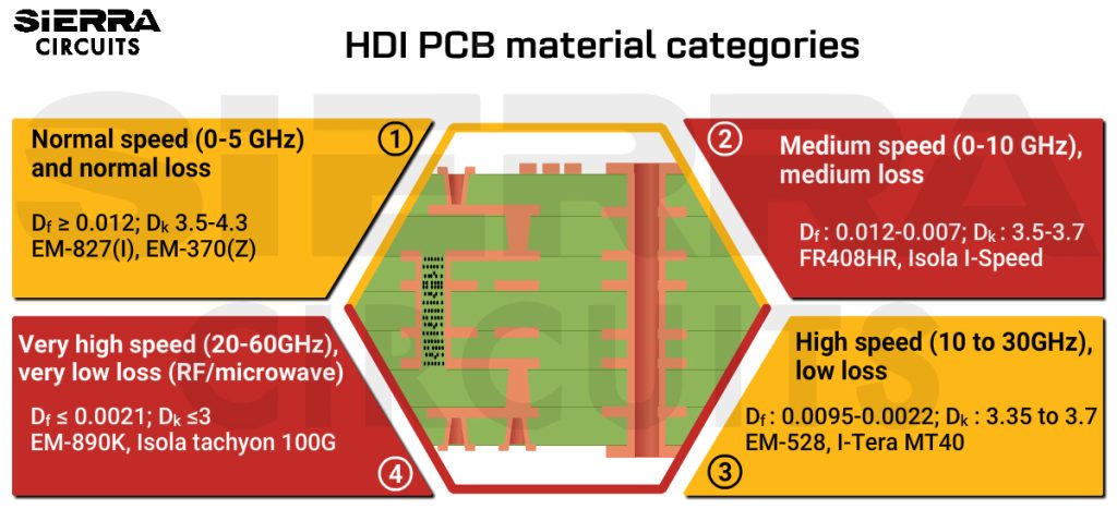
Choosing the right dielectric material for a PCB is important no matter what application you’re working. However, the stakes are higher with high-density interconnect (HDI) technologies.
HDI / Blind & Buried Vias
Via Filling Techniques Designers Need to Know for PCB Fabrication
PCB via filling is a technique in which the plated hole is filled with a conductive or non-conductive ... more »
PCB Manufacturing
Solder Mask Layer in PCBs: Top 4 DFM Guidelines
After PCB fabrication, the copper traces on the board typically face the risk of oxidation and corrosion due ... more »
PCB Manufacturing
How to Choose the Right HDI PCB Materials
Choosing the right dielectric material for a PCB is important no matter what application you’re working. However, the ... more »
HDI / Blind & Buried Vias
Via Filling Techniques Designers Need to Know for PCB Fabrication
PCB via filling is a technique in which the plated hole is filled with a conductive or non-conductive ... more »
PCB Manufacturing
Solder Mask Layer in PCBs: Top 4 DFM Guidelines
After PCB fabrication, the copper traces on the board typically face the risk of oxidation and corrosion due ... more »
PCB Manufacturing
How to Design Reliable Microvias in Your PCBs
Microvia failure occurs due to the thermal stresses that arise during the PCB assembly process. These stresses can ... more »
HDI / Blind & Buried Vias
How to Optimize Your PCB Designs for Testing by Harry Kennedy
Harry Kennedy, an electrical engineer and technical specialist at Altair, has shared his expertise in optimizing PCB designs ... more »
PCB Design
The Future of PCB Etching by Laurent Nicolet
Laurent Nicolet, the Vice President of Business Units Electronics at the Schmid Group, talks about the future of ... more »
PCB Experts
6 Common Solder Mask Errors Every PCB Designer Should Know
A solder mask is an insulation layer that covers conductive areas such as traces and pads. Inappropriate solder ... more »
PCB Design
Advantages of Ordering PCB Prototype and Bulk Production from a Single Fab House
Choosing the same fab house for PCB prototypes and bulk production has many advantages such as better DFM ... more »
PCB Manufacturing
How to Design and Build a Hybrid PCB Stackup
A hybrid stackup construction enhances your PCB’s performance and cost-effectiveness by combining different materials or technologies. It helps ... more »
PCB Manufacturing


Fabrication, Procurement, & Assembly. PCBs fully assembled in as fast as 5 days.
- Bundled together in an entirely-online process
- Reviewed and tested by Engineers
- DFA & DFM Checks on every order
- Shipped from Silicon Valley in as fast as 5 days

Fabrication. Procurement & Assembly optional. Flexible and transparent for advanced creators.
- Rigid PCBs, built to IPC-6012 Class 2 Specs
- 2 mil (0.002″) trace / space
- DFM Checks on every order
- 24-hour turn-times available

Complex technology, with a dedicated CAM Engineer. Stack-up assistance included.
- Complex PCB requirements
- Mil-Spec & Class 3 with HDI Features
- Blind & Buried Vias
- Flex & Rigid-Flex boards